
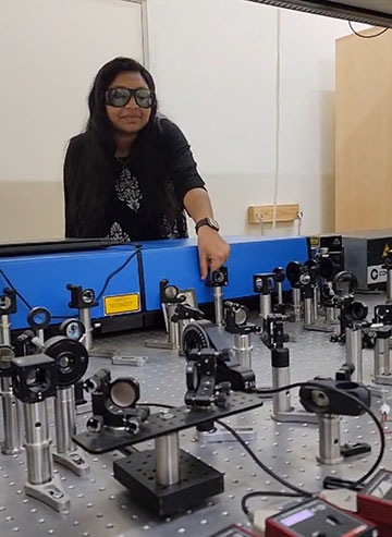
First author Jyothsna K Manattayil aligns the optical beams for up-conversion experiments. [Image: Harinee Natarajan]
Researchers at the Indian Institute of Science, Bangalore, India, have exploited a novel 2D material to fabricate a compact and efficient device for converting short-infrared light into the visible range (Laser Photonics Rev., doi: 10.1002/lpor.202400374). The miniaturized design opens up new possibilities for widefield infrared imaging, providing an efficient and practical up-conversion solution that enables high-performance silicon sensors to be used in place of cumbersome infrared photodetectors.
Turning to gallium selenide
Traditional techniques for frequency up-conversion rely on bulky nonlinear crystals and careful optical engineering, while emerging alternatives with a smaller form factor struggle to provide high conversion efficiencies. To combat those problems, the researchers instead turned to gallium selenide (GaSe), a layered semiconductor with a nonsymmetric structure known for its ability to generate higher harmonics.
In their design, the researchers leverage a thin flake of multilayered GaSe as the active layer in a nonlinear optical mirror, separated from a reflective gold surface by a dielectric spacer. When an input infrared signal with a wavelength of around 1550 nm is combined with a pump laser at 1040 nm, optical mixing within the 2D material produces 622-nm light through a process called sum-frequency generation (SHG).
“This process is coherent, which ensures that the properties of the input beam are preserved at the output,” explains corresponding author Varun Raghunathan. “If one imprints a particular pattern in the input infrared frequency, it automatically gets transferred to the new output frequency.”
Captured up-conversion
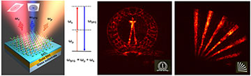
High-fidelity infrared images can be captured by combining a compact solution for frequency up-conversion with a conventional silicon-based sensor array. [Image: Jyothsna KM]
The researchers enhanced the strength of the SHG signal by optimizing the thickness of the layers. With a 45-nm flake of GaSe attached to a 50-nm dielectric layer, they achieved a 40-fold improvement over a reference structure with a wider spacer layer and no back reflector. The performance of this optimized structure matches that of state-of-the-art up-conversion schemes, while similar efficiencies can be achieved at other infrared frequencies by altering the thickness of the layers.
To show that the miniature device can be used for widefield infrared imaging, a pattern encoded in the input signal was projected onto an extended area of the GaSe flake. Capturing the up-converted output with a conventional silicon-based camera produced high-fidelity images in both real-plane and Fourier-plane configurations, while real-time filtering operations could also be performed through Fourier-domain processing.
The researchers are now working to improve the efficiency of the up-conversion process still further, which they believe could be achieved by using a higher pump power, combining multiple GaSe flakes within the stack or integrating resonant structures into the device design.