
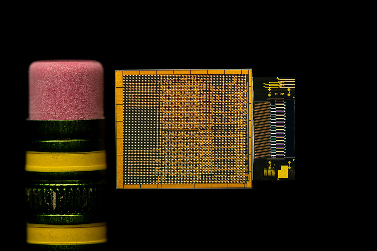
The optical compute interconnect (OCI) chiplet of Intel’s Integrated Photonics Solutions Group, shown next to a pencil eraser. Intel says the chiplet is “expected to enable massive AI infrastructure scalability.” [Image: Intel Corp.]
The recent surge in generative AI—and the voracious appetite for data of the large language models (LLMs) behind it, such as GPT-4—have raised the threat of bandwidth bottlenecks and soaring energy costs for data centers. Solving those problems would seem to have the makings of a “killer app” for silicon photonics. In principle, the latter can help address AI’s emergent bandwidth issues through schemes that let data stay encoded as fast, energy-efficient light all the way up to the “point of compute” (the electronic GPU or CPU)—all while taking advantage of the cost and manufacturing efficiencies enabled by the existing, mature CMOS infrastructure.
A bevy of startups and early-stage ventures, such as Ayar Labs, Celestial AI and Lightmatter, are attempting to build businesses around just that sort of opportunity. Amid that youthful bustle, however, more established firms in the semiconductor and networking businesses have hardly been standing still.
Most recently, the semiconductor giant Intel Corp. has provided new details on its own optical compute interconnect (OCI) chiplet. Intel argues that its chiplet—a prototype silicon photonics product originally demo’d at OFC 2024, and currently being trialed as an optical I/O solution with selected customers—“represents a leap forward in high-speed data transmission.”
Generative AI’s data bottleneck
In a press preview, Thomas Liljeberg, senior director of product management and strategy at Intel’s Integrated Photonics Solutions Group, summed up the data-transmission problem by first pointing to the extraordinary growth of the LLMs underlying generative AI. In recent years, he observed, the size of such models has mushroomed by, on average, an order of magnitude every 18 months. And that has created the need to “move a lot more data … over much larger clusters,” at all scales.
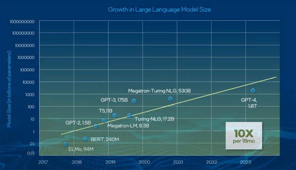
In its press presentation, Intel highlighted the explosive growth in the size of the large language models (LLMs) underlying generative AI. [Image: Intel Corp.]
With data passing between memory modules and GPUs or CPUs through conventional copper interconnects, the exponential growth of data transfer means that current systems are “invest[ing] more and more power into the [electrical] I/O versus into the compute part of the resource,” Liljeberg said. “And, of course, the compute is what we can use to solve the AI model at hand or monetize it in the business.”
Intel’s OCI chiplet
As with some products being pursued by other companies, Intel’s newly unveiled OCI chiplet attempts to reduce this “I/O tax” by bringing the optical I/O subsystem, and the conversion between the optical and electrical domains, right up to the edge of the GPU or CPU doing the computational heavy lifting.
The new Intel chiplet is, according to Liljeberg, a “compact, fully self-contained I/O system” that combines two copackaged chips. One is a photonic integrated circuit (PIC) embedding waveguides, amplifiers and integrated indium-phosphide-based lasers supporting dense wavelength-division multiplexing (DWDM). The other is an electrical integrated circuit (EIC) with control circuitry and drivers. The result, said Liljeberg, is an I/O subsystem that “connects to the I/O port on your CPU or GPU, converts [the electrical signal] into an optical signal that can travel over fiber, and is converted back on the other end.”
In the OFC 2024 demo, Intel showed off the chiplet’s datacom chops in a 4-terabit-per-second (bidirectional) connection between CPUs. The setup leveraged eight fiber pairs with eight wavelengths per fiber, or 64 lanes in all, each with a 32-Gbps data rate in both directions. The overall power efficiency was 5 pJ/bit.
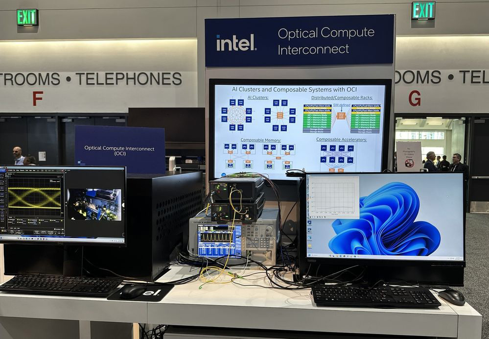
Intel demonstrated the OCI chiplet in its booth at OFC 2024. [Image: Intel blog posting]
“You can think of it as 4-Tbps connectivity in a 10-W envelope, so it’s very, very efficient,” Liljeberg maintained. “And as we scale to more bandwidth, the advances only grow; it’s a performance that scales very well.”
He also highlighted “a number of knobs to turn” to achieve that scaling in the future. These include increasing the number of wavelengths per fiber connection from the current 8 to 16 or 32; boosting the line rate past 32G (perhaps via interconnect protocols beyond the current standard, PCIe gen5); and increasing the number of fibers attached to the chiplet. The combination of those variables, Liljeberg argued, means that “we have at least five or six generations of doubling-up on bandwidth, with the same core technology,” which “gives us confidence that we’re heading down a healthy path.”
The laser-on-chip advantage
Intel is, of course, not alone in recognizing the need to solve generative AI’s I/O conundrum—or in offering a silicon photonics chiplet as part of the answer. But in the race to serve this market, the company believes it has a number of advantages. One of the biggest, the firm says, is Intel’s demonstrated ability to integrate reliable lasers directly into silicon chips at scale. The firm points out that, for the pluggable-transceivers market, it has shipped “more than 8 million PICs with over 32 million on-chip lasers,” with “industry-leading reliability.”
In a follow-up interview with OPN, Liljeberg listed some of the reasons that integrated on-chip lasers are a big deal for I/O applications. One is the dramatic reduction in coupling loss, a persistent headache for external lasers hooked into chips via fiber connections. “When you’re in a use case where the goal is the absolute best power efficiency,” Liljeberg said, “it’s really illogical that the first thing you do after generating light is to throw at least half of it away before you even start doing anything.”
In Intel’s view, one of its biggest advantages in serving this market is the firm’ demonstrated ability to integrate reliable lasers directly into silicon chips at scale.
Putting the laser on chip also makes sense, he added, because it means the chiplet becomes “a complete optical subsystem.” That has advantages from the point of view of cost-of-production and quality control—particularly as the lasers are integrated at wafer scale. “That’s an important distinction,” Liljeberg told OPN. “We’re not building a laser and then attaching that onto the silicon photonics platform. We’re attaching gain material onto waveguides [in silicon] and building the laser from that.”
More broadly, Intel believes that expertise in integration, at multiple scales, will be another key to winning in this market. That embodies integration of the silicon photonics components themselves; in the press event, Liljeberg pointed out that the initial OCI chiplet configuration has “more than around 2,000 [integrated] components … which I believe is state of the art for this kind of silicon photonics.” But it also extends to expertise in packaging—both the ability to construct “complex die stacks” of multiple components to put together the optical and electronic chips into a single optical I/O subsystem, and the integration of that subsystem into the compute platform. “You need to bring to bear all these disciplines and all these capabilities along the value chain,” he said.
Toward deployment
Right now, Intel’s OCI chiplet is at the prototype stage, and the company says it’s “working with select customers to co-package OCI with their SOCs [systems on a chip] as an optical I/O solution.” While he wasn’t able to name specific partners, Liljeberg suggested to OPN that the projects were taking place along two “parallel paths.”
One, with a somewhat shorter time horizon, is to look at how the chiplet can be attached to “either what exists already or is in flight already,” for deployment in applications like optimizing pooled computational resources. The other is to see how far the chiplet’s bandwidth density and performance parameters can in principle be pushed in the future. That’s something that will require a degree of “codesign or informed parallel design” with the CPU, GPU or SOC the chiplet is being attached to, and thus will require a longer timeline.
From pluggables to chiplets
One gets the sense that, as it eyes these future prospects, Intel is also mindful of its past. In the press event, Liljeberg stressed that the current chiplet offering is built on “20-plus years of silicon photonics R&D,” and eight years of experience in providing silicon photonics–enabled pluggable transceiver modules for the data center network business. Intel actually exited the pluggable-module business at the end of 2023, but it still plays in the market by providing silicon photonics chips and chipsets to module vendors.
“Since we shipped our first pluggable, we knew that one day, this is what we’re going to be doing,” Liljeberg told OPN.
Meanwhile, Liljeberg and others at Intel believe that the firm’s experience in silicon photonics for pluggables has set it up for success in the different, more dynamic current project of boosting bandwidth for generative AI. “Since we shipped our first pluggable, we knew that one day, this is what we’re going to be doing,” Liljeberg told OPN. “And I think we have spent these eight years with pluggables to really get ready for this.”
While AI is “not the only area” where optics can play a role, it’s “certainly super-exciting,” Liljeberg said. “There’s a huge opportunity to contribute in a meaningful way to that scaling that is happening, and not just sort of ride along.”