
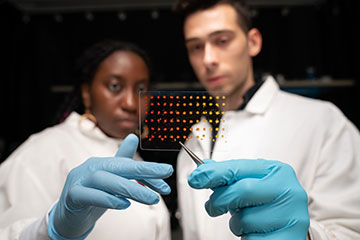
MIT researchers, including Eunice Aissi (left) and Alexander Siemenn, have developed an automated computer-vision process that can determine key properties of printed material samples quickly and accurately. [Image: Bryce Vickmark]
Researchers at the Massachusetts Institute of Technology (MIT), USA, have created a high-throughput analysis process that exploits computer vision to determine the band gap and stability of newly synthesized semiconductor materials (Nat. Commun., doi: 10.1038/s41467-024-48768-2). They say that by using algorithmic methods to analyze images of samples produced with rapid printing techniques, the automated approach significantly speeds up the assessment of candidate materials for applications such as solar cells, transparent electronics and next-generation batteries.
Playing the numbers game
Accelerating the discovery of new materials has become a numbers game, with engineers using ink-jet printing and other rapid synthesis techniques to produce thousands of samples based on chemical formulations suggested by AI search algorithms. The bottleneck now lies in the evaluation of the printed materials, since their droplet-like morphologies typically require a domain expert to measure key properties and performance indicators one sample at a time.
In contrast, the computer-vision tools developed at MIT can analyze hundreds of printed samples every hour in a scalable and parallel process. The researchers demonstrate their approach using perovskite materials being developed for future solar cells, first using a robotic printer to deposit around 200 samples with slightly different chemical compositions onto three separate slides.
To estimate the optical band gap of the samples, the team scanned each slide with a hyperspectral camera, with an automated segmentation process able to produce detailed reflectance data for each sample on the slide at the same time. Another algorithm then computed the optical band gap from the hyperspectral data extracted for each sample, with the calculated results matching an expert's manual assessments with an accuracy of 98.5%.
The computer-vision tools developed at MIT can analyze hundreds of printed samples every hour in a scalable and parallel process.
Fast and accurate
Conventional optical imaging was then used to determine the stability of the samples over time, exploiting the fact that perovskites change color as they degrade. In three separate experiments the samples were exposed to variations in light, humidity and temperature, with images taken every 30 seconds over a two-hour period. Using another computer-vision tool to calculate the level of degradation from the change in color, the automated process produced estimates that agree with expert evaluation to an accuracy of 96.9%.
“We were constantly shocked by how these algorithms were able to not just increase the speed of characterization, but also to get accurate results,” comments first author Alexander Siemenn. “We envision this slotting into an automated materials pipeline we're developing in the lab, using machine learning to guide where we want to discover these new materials, printing them, and then characterizing them, all with very fast processing.”