![]()
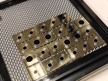
An infrared sensor made from germanium offers high responsivity over a wide spectral range. [Image: Aalto University / Xiaolong Liu]
Researchers at Aalto University, Finland, have demonstrated that an infrared photodiode made from germanium can collect 35% more light at the key telecoms wavelength of 1.55 µm than previous devices (Light. Sci. Appl., doi: 10.1038/s41377-024-01670-4). The nanoengineered sensor, which can be fabricated using standard manufacturing processes for silicon electronics, offers a high-performance solution that is also affordable for mass-market applications.
A dielectric layer
While photodiodes made from germanium are cheaper and easier to manufacture than those made from compound semiconductors, existing devices are much less efficient at capturing infrared light. Their response is also strongly dependent on the wavelength, which makes it difficult to enhance their performance through the use of anti-reflection coatings.
The team in Finland has previously shown that the absorption of light by these devices can be improved by nanostructuring the germanium surface with a needle-like pattern. This nanostructure gradually alters the refractive index close to the surface, ensuring that more of the incident light is transmitted into the germanium. The needle-like structure also scatters some of the incoming photons, which enhances the collection of light at longer wavelengths.
However, these nanostructures have proved challenging to integrate into practical photodiodes, since the larger surface area introduces electrical losses that compromise the optical response. To avoid that problem, the researchers have reimagined the device design, adding a highly charged dielectric layer on top of the nanostructure. This layer induces a strong electric field within the upper region of the germanium, providing a low-loss mechanism for separating and collecting the charge carriers generated by incoming photons.
Boosting efficiency

High-performance germanium infrared photodiodes. [Image: Aalto University / Xiaolong Liu]
Tests of the device show that it achieves a light-conversion efficiency of 92% at a wavelength of 1.55 µm, compared with 68% for a commercial germanium photodiode and 88% for the best-performing sensors made from compound semiconductors. The device maintains its response over a broader spectral range than any of the commercial devices, with the quantum efficiency remaining above 80% over wavelengths ranging from 0.2 to 1.7 µm.
The researchers also report that the background noise in the device, as measured by the dark current, is lower than has previously been achieved for germanium photodetectors. Combined with the enhanced conversion efficiency, this noise reduction improves the ability of the nanoengineered device to detect low light intensities. While not yet approaching the sensitivity of photodiodes made from compound semiconductors, this significant upgrade to the optical performance is likely to open up new applications for low-cost sensors operating in the near infrared.

