
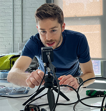
Rob Devlin. [Image: Courtesy of Metalenz, Inc.]
The July/August 2023 issue of Optics & Photonics News featured the magazine’s biennial feature spotlighting 10 Entrepreneurs to Watch. Here, we offer an interview with one of those entrepreneurs, Rob Devlin, a cofounder of Metalenz, Inc., a Harvard University, USA, spinout that is commercializing ultrathin metasurface components for mobile devices, consumer electronics and more.
Maybe we could start out with the “elevator pitch” on Metalenz—how would you sum up, in a few sentences, what the company’s doing and where you’re looking to take it at this point?
Rob Devlin: I think the big thing that you can do with metasurfaces, and what we can do at Metalenz, is to take advanced forms of optical sensing and simplify and shrink them to a price point and a form factor that’s compatible with mobile and consumer devices. This could be everything from 3D sensing, which is where we’ve launched our products today, to things like medical imaging or taking a piece of scientific equipment and putting it in the palm of people’s hands and cellphones.
Our focus had been really on this 3D sensing market. But what we’ve been doing recently is taking the same mass-production capability that we’ve developed—where we can make optics in the semiconductor foundry—and applying that to polarization imaging. This is something that’s typically been kind of a niche form of imaging for scientific and medical applications. Now we’ve launched a product, which we call PolarEyes, where you can do complete polarization imaging at a form factor and a price point where you can put this into basically any device out there.

When OPN talked with you in June 2022, you were awaiting your Series B funding, which I guess dropped in October. How are you using that money?
There’s a couple of places where we’ve been using it. One of the first uses has been to actually ramp up our production. You know, we’ve been building out an ops team as well as our supply chain to make sure that we can deliver these metasurfaces. So now we have a second foundry that we’ve brought up that’s in mass production with our optics.
But one of the biggest places we’ve been applying this is actually building out more of a machine-vision and computer-vision team. With metasurface optics, you essentially are able to do things that you can’t do with conventional optics. You can manipulate light in ways that you couldn’t otherwise. So we’ve been focusing on actually building systems and algorithms around the unique capabilities of these optics.
That comes back, again, to some of the products that we’re now launching, like PolarEyes. We actually have computer-vision and machine-vision teams that are taking that information that we can bring into the system, and starting to build up algorithms to do things like secure biometrics, vital-signs monitoring or other types of applications. So really, it’s about building the system-level capability and the team that can work not just on the optics but on all of the algorithms and software.
When we last talked, I think the company was at 22 people.
We’re at about 36 people now. So we’ve had quite a bump, and it’s largely been through this this most recent [Series B] fundraising round.
Let’s talk about the current product mix. Looking at your website, there’s I saw three product lines—Orion, Gemini and PolarEyes. Could you talk about those at a high level, and how they fit together in your strategic vision for Metalenz?
Sure. Orion is our first-generation product. That’s what we actually have launched into the market now; it’s in consumer devices today. And that’s primarily focused around 3D sensing. One example is dot-pattern projectors, structured light—the array of dots that gets projected onto your face every time you open your iPhone, for instance. Orion takes that system, which normally requires three or four lenses, and shrinks it down into a single metasurface optic.
“With metasurface optics, you essentially are able to do things that you can’t do with conventional optics.”—Rob Devlin
So that’s where we focused to get the technology out there. That’s also where we then brought up these foundry partners. But it just uses the base technology—it’s really a replacement, with a substantial reduction in system complexity, for existing optical modules.
How about Gemini?
Gemini is sort of the next logical evolution—where, with metasurfaces, you can encode multiple functions into a single optic. Normally you have one optic, and you get one function—your eyeglasses, for example, are typically just doing one thing. With a metasurface, you can actually put multiple functions into a single optic.
So Gemini is looking at expanding the applications of 3D sensing on the illumination side, where you can actually project out multiple patterns from a single metasurface. And the way we do that is actually by encoding a polarization response into the metasurface—you hit the metasurface with polarization A and it does one thing; you hit it with polarization B and it does something completely unique and independent.
So with Orion, we’re essentially combining multiple optics into one metasurface. If you go to Gemini, you’re taking multiple different optical modules—you would normally need two completely independent stand-alone illumination modules to do this—and we’re combining those into a single metasurface.
And what about the most recent product development, PolarEyes?
PolarEyes is in that same natural evolution, working on the imaging side of things. With PolarEyes, we are taking a complete polarization image of the scene that you’re looking at.

Standard lenses are really just capturing the intensity information. But you sometimes want to get at the polarization information, too, because that tells you a whole lot about the material and molecular makeup of an object; it can even tell you if what you’re looking at is natural or man-made. Polarization cameras actually do exist today, but they typically are something like 100 millimeters in size and often cost something like US$500.
With PolarEyes, using a single metasurface, we can completely parse out all of the polarization information that’s being reflected back off of the scene. So it gives you that additional information that your conventional lenses are typically throwing away. It’s a step beyond Gemini, in the sense that Gemini is working on two polarizations; with PolarEyes, you’re getting the complete polarization picture of everything that that you’re looking at.
Are there other things we should be looking for in the future in terms of products or R&D from Metalenz—another generation that we should be looking forward to?
We’re looking at places where we can go take this capability of polarization sensing and imaging, and use it not just for things like biometrics, but also for things like vital-signs monitoring. This is a case where using that polarization information allows you to possibly sense things and do things that you couldn’t otherwise.
The other place where we see the company expanding and technology moving is in the ability to make this work across the visible spectrum. Everything we’ve talked about so far has really been focused around these narrowband-type applications. But we also have the capability now to start moving toward some full-visible imaging applications, again not just through the design of the optic itself but also through the algorithms and software that we couple with the metasurface.
I want to switch to a few questions on your journey as both a scientist and an entrepreneur. I’m curious about when you first started getting interested in science and particularly in optics.
The place it really started for me was working with my grandfather, actually. He was in the Navy, and he was a radio operator. And after his career in the Navy, and serving in World War II, he took that passion, and was an electrical engineer by training, not necessarily by education. And he used to build and design radios in his basement.
“The place it really started for me was working with my grandfather … [H]e and I used to work together, putting … shortwave radios together. I’d say that was the very first spark where there was this idea: You could take these components, slap them together, and then all of a sudden you were hearing someone halfway across the world.”—Rob Devlin
So he and I used to work together, putting these shortwave radios together. I’d say that was the very first spark where there was this idea: You could take these components, slap them together, and then all of a sudden you were hearing someone halfway across the world. It was a cool realization—you don’t see any of the radio waves going out there, and you don’t necessarily have that direct physical connection. But if you put the components together the right way, all of a sudden, you’re able to interact and communicate with someone.
That generally set me in the direction of engineering, and wanting to do something in engineering. I started out in electrical engineering, again mainly looking at signal processing. And from there, I also got interested in how you could use materials to design new components—getting at things one layer deeper. That led me to go into materials science for a master’s; and, from there, metamaterials and metasurfaces is kind of the perfect combination of those two fields. Because in a metamaterial or metasurface, you’re trying to manipulate some sort of a signal by making a designer material.
And whether you’re working with radio waves or with visible or infrared light, it’s that same idea with a metasurface. A lot of the stuff that we do, we can’t really see. But at the end of the day, by putting things together in a proper way, you all of a sudden have this connection, this new information from the world you’re looking at. We’re working with something much smaller than resistors in a radio at this point; we’re working with nanostructures. But at a fundamental level, it comes down to the same thing.
From there, how did you come to found Metalenz?
I was doing my Ph.D. in the group of Federico Capasso at Harvard, the group where a lot of the foundational work on metasurfaces really started, going back to 2011. In Federico’s group I was focused mainly on finding ways to improve the performance and manufacturing of these metasurfaces, to get them to the point that they could really be useful for practical applications. Up to that point, there had been a lot of beautiful work on metasurfaces, and the exciting things they could do … but overall, the devices tended to be pretty inefficient in getting the light to go where you actually wanted it to go. And often the materials were still using metals, which wasn’t really going to transferrable to the semiconductor foundry.
So during my Ph.D., we got to the point where, in 2016, we had a process design capability that let us finally get to the 85-90% efficiency range for these devices. In that same year we showed the first really high-quality images with a metasurface. And we published a paper that ended up on the cover of Science.
At that point, I was really still thinking of going the academic route; Federico and I weren’t necessarily thinking about a company. But from that paper—just the amount of cold calls we started getting from cellphone manufacturers, from people in the optics industry, from entrepreneurs and investors asking us what we're going to do—we said, Well, it’s probably time now to see if this can be more than nice papers and research. It’s time to spin it out. And we did that in 2016.
You say initially you were thinking of an academic career and not really considering a career in industry. You’ve been at it in industry for a few years now. How have you found that transition?
I think one of the great surprises for me has been how much more challenging industry can be than when you’re doing something in research—but also how much more connection you’re able to have with other people.
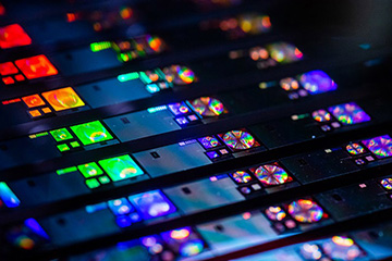
Metalenz is working on commercializing metasurface technology to enable new kinds of optical functionality—such as the company’s emerging PolarEyes polzarization-imaging product. [Image: Courtesy of Metalenz, Inc.]
Of course, in the academic world, there are collaborations, and you have colleagues or other people in the lab that are helping out. But to make an actual product, where you’re getting that to a consumer, all of the people in different specialties that you have to make sure collaborate together—that has been a really great part of being in industry. It’s kind of mind boggling when we sit back and think about just how many people touched a product in different areas, in order for it to go from the design phase all the way to something that’s going to be in a consumer device.
At the same time, I do think a Ph.D. really does prepare you for that. Because you have these open-ended questions. It may be that you’re applying it with a slightly different mindset when you’re looking at it for a product versus just pursuing knowledge for the sake of expanding knowledge. But at the same time, the ability to deal within uncertainty and open-ended questions that you get in a Ph.D. and in doing something in science—I think that all translates quite well to industry.
In the past year, Metalenz has snagged a couple of really notable awards—the Prism award at Photonics West, for example, and an innovation award from Laser Focus World; both of those were for PolarEyes. Could you talk a bit about the impact of recognition like that for a company at the stage Metalenz is at?
It’s definitely been really great to see. When you’re first launching a product, especially when you’re trying to do something that is very new, that’s exciting in itself. But at the same time, you want to make sure that you’re not just kind of caught up in your own hype cycle … Industry-focused awards like that kind of help you get a sense you’re heading in the right direction. And also, of course, from the point of view of connecting with customers and other folks, it has allowed us to really get the word out there and build up the traction for PolarEyes for the second generation of our technology.
You’ve had a lot of success in developing funding and interest in your company. What are the big lessons that you’ve learned during this process? If you were talking to someone just getting started, what would you tell them?
I think one of the biggest things is to have a very open mind. When we first started the company, for example, we weren’t necessarily thinking about 3D sensing as the place that metasurfaces would apply first. We really thought that the full visible spectrum was going to have to be developed for this to be an end product.
But as we went around and kept an open mind, rather than trying to force the technology into a particular market, we found the right product market fit with what we were doing. We made sure we were solving real pain points, not just having a really cool technology.
“[O]ne of the biggest things is to have a very open mind … I think the other thing, too, is not overlooking the mass-production side of things, from the very beginning.”—Rob Devlin
I think the other thing, too, is not overlooking the mass-production side of things, from the very beginning. There are examples of really interesting, really cool technologies from universities that never realized their full potential, because in the end there wasn’t a mass-production path for them, or they was too complicated, or something along those lines.
So you need to keep in mind that you don’t just want it to be interesting—you want to make it at the end of the day, and you want to be able to make it cost effectively, repeatedly, and so on. Getting some folks in the company very early on who had that industry experience, had some scars from having done it before, and a couple of gray hairs—that helped immensely with making sure that the technology actually found its way to market.
Are there any particularly big milestones for you looking back on your experience with this company—some things that set your pulse racing, or maybe some particular challenges that really stand out that you’ve overcome?
Coming back again to this idea of mass production, I think that a really cool moment, for me and for everyone at the company … was when we got the first 300-millimeter wafers with 10,000 of our devices on it that was made in a semiconductor foundry and a semiconductor fab.
You know, we had been going out and seeing the excitement from customers and other folks, and I think in general metasurfaces has been on kind of an upward trajectory in academia for a long time, where people were saying, This is ready for prime time. But then seeing the actual completed wafer from the fab, and seeing more devices on a single wafer than probably the Capasso group had made collectively in everyone’s Ph.D. work—that was one of those moments that was just really cool. Because now it was, Okay: It’s not just exciting and not just interesting. It’s real, and you can make it.
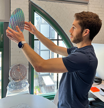
Rob Devlin, pictured with a semiconductor wafer containing Metalenz devices. [Image: Courtesy of Metalenz, Inc.]
In that in that same vein, I think one of the biggest challenges has been the chicken-and-egg problem. When you go and you start introducing a new technology to customers, they say, “This is great, this is fantastic. Show me something in mass production.” And then when you try to get a partner for mass production, they say, “This is great, this is interesting. Show me a customer so we can make sure we can invest.”
I think that was one of the biggest challenges, is trying to find the right partner and the right customer who could help us span that gap. And it has to be more than just interesting PowerPoint slides or prototypes that we would send out. At some level, people are putting their jobs on the line. So how much time and effort it took to get to get there, and making sure we kept moving forward on that—I think that was one of the big challenges.
You’re envisioning a very big future for Metalenz. What kind of timelines and ultimate market sizes, in the near and long term, do you talk about at the company?
In the shorter term, I think we see something like PolarEyes being on market in the next two years. And the first target is really around biometrics. But ultimately, when you bring new information to these systems, there’ll be a whole set of applications that can emerge that maybe we’re not even envisioning yet.
Then, over the 5- to 10-year range, as we move into doing things with the full visible spectrum, we can look at things like how we can use polarization for vital-signs monitoring and other applications.
As to market size, in the near term we think of it in the US$1 billion to US$10 billion range for the markets we could address with something like PolarEyes and Orion and the other technologies collectively. Ultimately, though, in the next 10 years, there’s going to be an even bigger emergence of computer-vision and machine-vision types of applications generally. So a US$30 billion to US$50 billion market, I think, looks really realistic at this point, as we look 10 years down the road.