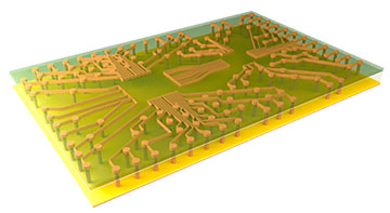
The new approach packages with glass instead of silicon. [Image: Schmid]
In late January, the Germany-based tech and manufacturing companies Trumpf and Schmid Group announced that they had partnered to develop an improved packaging manufacturing process for microchips. Ultimately, they hope to enable manufacturers to produce better electronic components at a lower cost with an advanced packaging process that uses glass for interposers rather than silicon.
Looking to lower costs
In advanced packaging, manufacturers combine individual chips and package them as a single electronic device, often using a silicon component known as an interposer as the substrate. However, silicon interposers are both expensive and complex. In an effort to reduce costs while improving the end product, Trumpf and Schmid have instead looked to leverage glass as an interposer.
“Advanced packaging with glass is a crucial future technology for the semiconductor industry,” says Christian Weddeling, business development manager at Trumpf responsible for semiconductors. “Glass is significantly cheaper than silicon. This will enable manufacturers to reduce production costs and make high-performance end devices much more affordable for customers.”
A delicate process
The companies’ proposed approach combines laser etching with wet chemistry—techniques that they say play to each of the partner’s respective strengths. “It is the combination of TRUMPF’s laser technology and the Schmid Group’s expertise in etching processes for microchip production that enables efficient production,” says Christian Buchner, vice president of Schmid’s photovoltaics business unit.
This process, however, does require a tremendous amount of precision and delicacy, as the glass is just 100 µm to 1 mm thick. To create connections on the interposer, holes must be drilled through the glass to create “through-glass vias”—and often manufacturers must make millions of such holes to get the connections they need. In a press release, the companies claim that their approach to wet chemistry “shortens process times by a factor of 10.”
First, a Trumpf ultrashort laser pulse is used to selectively change the structure of the glass. Next, the glass is treated with an etching solution, which creates holes in the desired locations. The holes are then filled with copper to form conductor tracks that provide electrical connections between the front and back of the glass substrate. “The laser and etching processes must be perfectly coordinated to create precise holes. Only through close cooperation between the two companies can we achieve the extreme levels of accuracy that are standard in the industry,” said Buchner.
Future growth
The collaboration is strategically timed for Trumpf and Schmid. Market analyst Boston Consulting Group predicts that the market for advanced microchip packaging will grow to more than US$96 billion by 2030, and the companies note in a press release that they believe that “advanced packaging with the help of glass” could be an important part of this increase in value.
While consumer electronics like smartphones currently dominate the advanced packaging sector, applications in artificial intelligence—another very hot market—are likely to drive growth in the future, according to the companies.
