
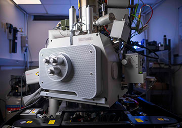
The scanning ultrafast electron microscope developed by Bolin Liao and colleagues at the University of California, Santa Barbara, USA. [Image: Matt Perko]
Researchers in the United States say they have visualized the behavior of photoexcited charge carriers as they cross the junction between two semiconductor materials, in this case silicon and germanium, for the first time (Proc. Natl. Acad. Sci. USA, doi: 10.1073/pnas.2410428121). By exploiting an ultrafast version of a scanning electron microscope, they create movies that reveal what happens when these so-called “hot” carriers diffuse and interact with the energy barrier at the interface.
Down to picoseconds
The high-speed dynamics of these photoexcited carriers have a direct influence on the performance of many optoelectronic devices, but it is challenging to track their behavior because they diffuse and dissipate on picosecond timescales. “When you excite charges in the uniform silicon or germanium regions, the hot carriers move very, very fast,” explains lead author Bilon Liao of the University of California, Santa Barbara. “The really exciting thing about this work is that we were able to visualize how the charges, once generated, actually transfer across the junction.”
The instrument developed by the team combines the surface sensitivity of a scanning electron microscope with an ultrafast pulsed laser that acts like a shutter operating in the picosecond regime. When a single optical pulse generates photocarriers in the semiconductor structure, the pulsed electron probe scans the surface of the material to capture a time series of contrast images that follow the evolution of photocarriers in both space and time.
The instrument developed by the team combines the surface sensitivity of a scanning electron microscope with an ultrafast pulsed laser that acts like a shutter operating in the picosecond regime.
Visualizing charge carriers
Using this technique, called scanning ultrafast electron microscopy, the researchers visualized the influence of the junction on both electron and hole transport. When the photocarriers are excited in the silicon, the team finds that the built-in potential at the interface attracts holes while pushing the electrons away, causing holes to accumulate at the interface and reducing the speed of the electrons.
In contrast, most of the photoexcited electrons produced in the germanium cannot migrate across the junction because of the large offset between the conduction bands of the two materials. While the potential barrier at the interface tends to push the holes away from the junction, the movies also show how some of the holes excited close to the interface can become trapped as they cross into the silicon.
Such charge trapping is known to affect device performance, particularly when the primary aim is to convert light into electricity, but this is the first time the process has been observed experimentally. “We didn't expect to be able to image this effect directly,” said Liao. “Our results have significant implications for applications where the efficient collection of hot photocarriers is desirable, such as photovoltaics and photocatalysis.”