
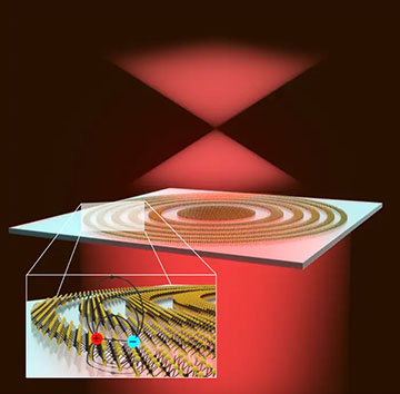
The lens, made of concentric rings of tungsten disulfide (WS2), uses excitons to efficiently focus light. The lens is as thick as a single layer of WS2, just three atoms deep. The bottom left shows an exciton: an excited electron bound to the positively charged “hole” in the atomic lattice. [Image: Ludovica Guarneri and Thomas Bauer, University of Amsterdam]
How thin can a lens get? When the lens consists of 2D semiconductors that use quantum effects to focus incoming light, it can be just three atoms thick.
Researchers in the Netherlands and the United States say they have built such a lens out of a monolayer 2D semiconductor metasurface (Nano Lett., doi: 10.1021/acs.nanolett.4c00694). The zone-plate lens design measures 0.5 mm across but only 0.6 nm thick. Excitons within the metasurface shape the wavefront of diffracted light.
It’s all in the material
The zone-plate lens consists of concentric rings of tungsten disulfide (WS2), which belongs to a group of 2D semiconductors called monolayer transition metal dichalcogenides, or TMDs. Scientists have multiple ways to manipulate the light scattering by excitons in such materials, which makes TMDs great candidates for nanophotonic systems.
A team based at the University of Amsterdam, Netherlands, and Stanford University, USA, used an exfoliation technique to build up a WS2 monolayer on a substrate of sapphire, and then the researchers etched the zone-plate pattern into the lens material. A structure only three atoms thick in one dimension cannot support itself, so it remains on the transparent substrate.
“The exact choice of transparent substrate (e.g. switching to quartz instead of sapphire) has a very subtle influence on the strength of the light–matter interaction, but this has no strong effect on the performance of the lens,” says Jorik van de Groep of the University of Amsterdam, one of the study’s corresponding authors.
The diameter of the zone-plate lens developed in this study is large compared with the size of monolayer TMDs created through conventional exfoliation techniques, according to van de Groep. Another member of the study team, Fang Liu of Stanford, developed a method called gold-assisted exfoliation to create a monolayer of multiple square millimeters. “This technique leverages an ultra-smooth gold film to selectively peel off only the first layer from a large bulk crystal,” van de Groep explains.
Testing the lens
According to van de Groep, the team’s biggest challenge was measuring the low-temperature lens performance in a controlled manner, with the equipment they had available.
The lens design was optimized for light with a wavelength of 615 nm. The researchers mapped the photoluminescence from the lens and found a clear peak at 2 eV, the characteristic excitonic emission of the material. The linewidth was 10 meV narrower than that of WS2 layers created through conventional chemical-vapor deposition. Cooling the zone-plate lens to cryogenic temperatures boosted the focusing efficiency of the monolayer TMD.
According to van de Groep, the team’s biggest challenge was measuring the low-temperature lens performance in a controlled manner, with the equipment they had available. “While measuring a reflection spectrum at cryogenic temperatures is relatively straightforward, performing a quantitative analysis of the intensity in the focus proved to be very challenging,” he says.
Future avenues
Next, the Amsterdam-Stanford team will try to achieve more complex optical functions with their atomically thin optical elements. They hope to control these optical functions with electrical voltages.
The research could lead to future augmented-reality (AR) glasses. “The projection of images in the user’s eye will require multicolor optical elements,” van de Groep says. “However, the very high transmissivity of the current lens could be interesting to extract a very small fraction of the light (in this case red) and project it on a camera/imaging system to extract information from the environment that can be used to determine what to project, without perturbing the user’s sight.” AR headwear made with TMDs might also require stacking of multiple materials with peak excitonic efficiency at different wavelengths.