

Alvaro Casas-Bedoya (left, holding the chip) and Ben Eggleton in the Sydney Nanoscience Hub at the University of Sydney Nano Institute. [Image: Stefanie Zingsheim, University of Sydney]
Researchers in Australia have developed a microwave photonic filter that harnesses an optical nonlinearity to process radio-frequency (RF) signals on a silicon photonic chip. The team integrated chalcogenide waveguides, which generate stimulated Brillouin scattering, into a previously manufactured CMOS chip to make a high-bandwidth electro-optic device (Nature Commun., doi:10.1038/s41467-023-43404-x). The technique could find uses in future aerospace systems and wireless networks.
Needed: Fine spectral resolution in a small package
In the race to miniaturize modern devices, scientists need tunable RF filters with fine spectral resolution that operate at frequencies higher than 30 GHz―and they need them to fit into tiny, low-power packages. Surface acoustic wave filters experience large losses in this range, while other types of RF filters are either too large to be integrated into silicon chips or cannot be tuned. Fortunately, stimulated Brillouin scattering, which was discovered a century ago and can provide the necessary fine spectral resolution, has regained interest since its first use in a photonic chip 12 years ago.
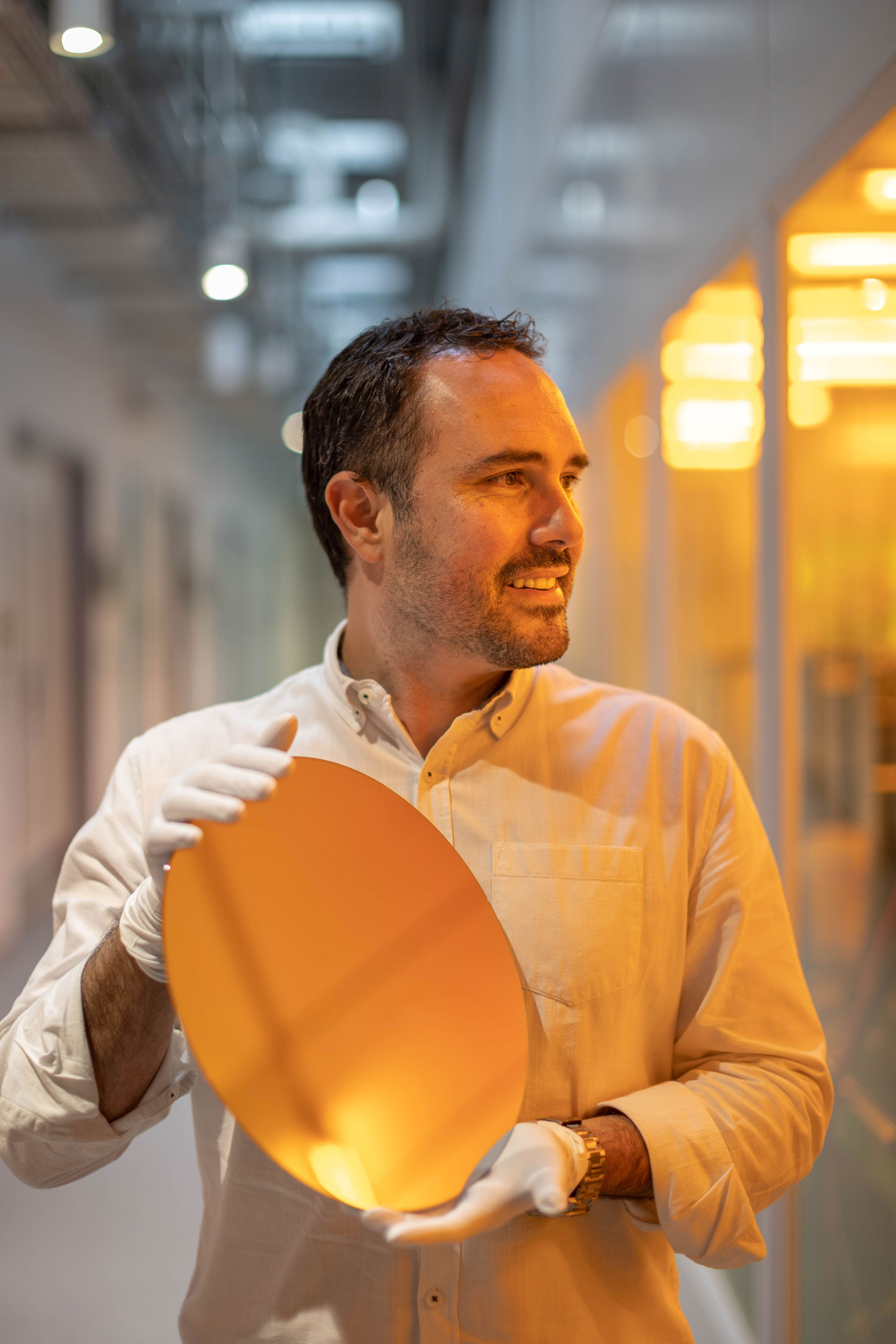
Alvaro Casas-Bedoya holds a silicon wafer used to manufacture semiconductors in the Sydney Nanoscience Hub at the University of Sydney, Australia. [Image: Stefanie Zingsheim, University of Sydney]
Improvements to the nanofabrication process and full integration of chip-scale components lower the optical losses and enhance RF link performance
Optica Fellow Benjamin J. Eggleton and his colleagues at the University of Sydney, Australia, devised Brillouin waveguides made with arsenic trisulfide and integrated them into a silicon photonic platform made in a standard CMOS foundry. The resulting filter takes the RF input and the modulating optical carrier―the beam from a 1550-nm laser―and passes it through tunable couplers and a phase shifter before routing it through the chalcogenide spiral waveguide, where the light and sound interact resonantly.
Lowered optical losses
All the silicon and chalcogenide components of the microwave photonic filter fit onto a 5 × 5 mm wafer, and the device demonstrated a spectral resolution of 37 MHz―a resolution already narrow enough for some real-world applications, according to Alvaro Casas-Bedoya, a member of the research team. Improvements to the nanofabrication process and full integration of chip-scale components lower the optical losses and enhance RF link performance, he adds.
“In this demonstration, the performance of the RF filter was constrained by the optical losses at the interface between different materials on the same chip,” Casas-Bedoya says. “These losses were introduced due to a post-processing step conducted within our cleanroom. This step was necessary to enable the hybrid integration.”
Next, Casas-Bedoya says, the Sydney group will improve the filter’s performance by exploiting the latest so-called “back-end-of-line” processes for integrating the different materials on the same chip. The scientists will also explore the uses of other materials such as lithium niobite and silicon nitride for improving the performance of the photonic circuitry.