
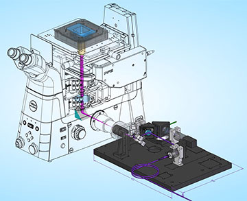
Researchers have developed an easy-to-build, low-cost 3D nanoprinting system that can create arbitrary 3D structures with extremely fine features. The method is compatible with most commercial microscopes. [Image: Cuifang Kuang, Zhejiang University]
Researchers in China have reportedly developed a low-cost 3D laser printing system that can fabricate structures with features only a few hundred nanometers in size (Opt. Lett., doi: 10.1364/OL.495286). The technique employs two-step absorption to create a variety of nanostructures, including 2D gratings with periods of less than 150 nm. The new method, which replaces two-photon absorption with a high-power femtosecond laser, could be used to create many optical components from metamaterials to microlenses.
From two-photon to two-step absorption
Scientists already know how to use nonlinear two-photon absorption to spark the photopolymerization process in 3D printing materials and create nano-sized features. However, the process requires an expensive—and finicky—femtosecond laser.
Cuifang Kuang, Zhejiang University, and his colleagues at took a more recent approach: harness two-step absorption to excite the photoinitiator molecules that drive the 3D printing process. Under the right conditions, two-step absorption demonstrates the same kind of nonlinear effect as two-photon absorption, but the 405-nm output from an ordinary CW laser diode—similar to the light sources in Blu-ray players—is sufficient to power the printing.
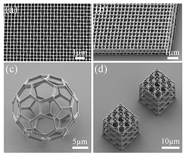
The researchers used their new system to make a variety of detailed 3D structures, including a 3D woodpile structure (top row), a 20-μm-diameter buckyball (bottom left) and two cubical box frames (bottom right). The images were acquired with an electron microscope. [Image: Cuifang Kuang, Zhejiang University]
The team used a 532-nm CW laser as the second source in the two-step absorption process. The experimental setup combined the beams with galvanometric and dichroic mirrors and focused them through an oil-immersion microscope objective onto the photoresist, which incorporated an organic compound called benzil as the photoinitiator. A piezoelectric stage controlled movement while the setup scanned the photoresist with the light beam.
Nanoprinting at low cost
With a scan velocity of 100 μm/s, the device produced 2D grating lines that were clearly distinguishable from each other at periods of 125 to 140 nm. The team also printed an eight-layer 3D woodpile photonic crystal with a lateral period of 350 nm, plus a “buckyball” structure just 20 μm across.
Even when the team boosted the scan velocity by an order of magnitude to 1000 μm/s, the setup produced distinguishable polymer nanostructures in two and three dimensions. The researchers noted that the action of the green 532-nm laser enhanced the polymerization process when higher scan speeds meant that less of the 405-nm laser’s power was getting to the photoresist.
“This new approach helps make 3D nanoprinting accessible to scientists, even ones who are not familiar with the optical systems typically used for this type of fabrication,” said Kuang in a press release accompanying the research. “It could eventually lead to low-cost desktop 3D nanoprinting devices that could offer precision nanoprinting to anyone.”