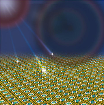
Researchers have developed a megapixel photon-counting camera based on single-photon avalanche diode (SPAD) image sensors, which can reportedly capture images in faint light at unprecedented speeds. [Image: Arianna M. Charbon, Kazuhiro Morimoto, Edoardo Charbon]
Researchers in Switzerland and Japan have reported a breakthrough in speed and accuracy for an imaging sensor based on a large-format array of single-photon avalanche diodes, or SPADs (Optica, doi: 10.1364/OPTICA.386574). The team believes the sensor could find numerous applications in industrial and scientific research applications.
The speed and detail possible with the new camera technology, the researchers say, make it ideally suited for quickly capturing detailed 3D images, as well as 2D images of scenes with high dynamic range (HDR). It may be useful, they suggest, for boosting the accuracy of lidar for autonomous cars and imaging detail in robotics, augmented reality and security applications, as well as for advanced capabilities in biomedical and quantum imaging.
A megapixel array
The camera comprises a record 1-megapixel array of SPADs, explains co-author Edoardo Charbon of the Advanced Quantum Architecture (AQUA) laboratory at Switzerland’s Ecole Polytechnique Fédérale de Lausanne (EPFL), where the sensor was designed. It detects single photons and converts them into electrical signals that are stored in a digital memory at a rate of about 150 million times per second. The SPADs are time gated to give the camera a “shutter speed” that allows light into each sensor for as little as 3.8 ns, and the device can acquire images at up to 24,000 frames per second.
In SPAD research, achieving a megapixel SPAD sensor has been considered an important milestone for more than a decade, according to Charbon. The breakthrough implementation of the first SPADs in CMOS technology, around 2003, triggered the implementation and design of large SPAD imagers, potentially manufactured in volume at affordable prices, he says. Indeed, there are versions of SPAD imagers available today in many smartphone cameras and other household devices.
An old dream, realized
Citing previous work from his laboratory, Charbon says, “We saw that our ¼-megapixel camera was having traction in the imaging/microscopy community, while researchers were asking for more pixels and potentially smaller ones. We had among the best SPADs in terms of noise and sensitivity, and we thought we could realize an old dream”—a megapixel array.
The first problem to solve was the pixel, Charbon says. “At the time our pixel was 16 µm in size and we knew that a reduced pixel meant shrinking the SPAD down to a very small diameter,” he says.
Scaling down so radically was uncharted territory, Charbon says. “In addition, given that our best CMOS technology for SPADs has a feature size of 180 nm, we could only afford seven transistors per pixel. So, we started being creative and shared every structure we could, including three transistors, among clusters of 2×2 pixels. This yielded a configuration with 5.75 transistors per pixel. To the best of our knowledge, this is the smallest number ever achieved in a gated SPAD pixel,” he says.
Further innovation, Charbon says, could pave the way to a new generation of photon-counting cameras for photography, featuring ultra-low-light imaging capability, global shutter function, and on-chip AI-based image processing.
Imaging from light to dark
Charbon notes that the new camera’s high dynamic range—its ability to distinguish a wide span of values from light to dark—could be especially important, in applications like automotive imaging and lidar, for situations like entering or exiting a tunnel. Also, for cars, much wider fields-of-view from onboard cameras could increase safety through more extended periphery vision in day and night driving conditions, he says.
“Surveillance is another application field requiring HDR, for example, for monitoring in direct sunlight,” Charbon says. “HDR vision can also be important in situations of low or impaired visibility due to high scattering—whenever high illumination usually fails to achieve good enough contrast,” he says. Facial recognition is an obvious application of this technology, he adds, but not profiling, which requires micrometric precision in depth.
Researchers see wide application space
Other applications of the megapixel SPAD imager, Charbon says, could include studies in robotics, in which a large-format, time-resolved camera could build an extraordinarily detailed view of a scene in 3D. These could help the robot navigate complex environments by taking an image and “memorizing” it. Complex trade-offs could be found in reconstructing these scenes, he says.
“In science, one could reproduce astronomical phenomena where light appears to propagate faster or slower than the speed of light,” Charbon says. What’s more, “the technology is potentially applied to imaging ‘around the corner’ or ‘behind the objects’. In biomedical imaging, widefield lifetime fluorescence imaging microscopy could reach unprecedented levels of detail over a large field-of-view.”
Charbon also sees potential for imaging with a large number of SPADs in other applications, such as quantum computing. For now, however, he believes the most immediate applications probably lie in AR/VR and automotive sensing—and, perhaps, in niche applications for smartphone cameras and high-end cameras for photography.

