
![]()
Silicon carbide (SiC) crystals. [Image: Getty Images]
Halo Industries, a Stanford University spinoff company developing and marketing a laser-based process for producing silicon carbide (SiC) semiconductor wafer substrates, announced that it had raised “up to US$80 million” in an oversubscribed Series B funding round led by investor Thomas Tull’s US Innovative Technology Fund (USIT). Halo says it will use the new cash to help “scale the commercialization and reach of its technology and advance its mission to establish the new gold-standard of silicon carbide substrate production.”
A promising but tough material
Halo’s prospects rest on the enormous promise of SiC—a wide-bandgap (WBG) semiconductor key to the much-sought-after electrification of society. Among other virtues, WBG semiconductors sport a high breakdown voltage, which can translate into devices with better efficiency, faster switching and improved heat dissipation relative to silicon-based devices. These favorable qualities have made SiC particularly attractive for so-called power electronics used in electric vehicles (EVs), solar and wind power, grid and charging infrastructure, and other applications.
But SiC has its disadvantages. For one, it’s costly stuff, which puts a premium on preserving as much of the material as possible during processing. It’s also brittle and tough to work with, with a hardness approaching that of diamond, which makes it easy to waste material when conventional saw technology is used to do the cutting. As a result, photonic and laser-based techniques have become increasingly important in the SiC manufacturing chain (see “Photonics for Processing Wide-Bandgap Semiconductors,” OPN, May 2024).
Lasers to minimize waste
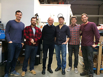
Halo Industries founding team, circa 2016. [Image: Halo Industries]
Against that backdrop, Halo—spun out of a Stanford University lab in 2014, and now based in Santa Clara, CA—claims to have developed a proprietary, multi-step laser-based process that the firm says can “significantly increase yield” of SiC while “minimizing waste and production cost” relative to mechanical and thermal processes.
At present, the firm maintains it offers “industry-best wafer-per-ingot yield” in SiC. Halo also maintains that its processes cut “the number of performance-sapping defects” and warping effects in SiC wafers, minimizing the need for post-processing and enabling “a new quality standard” for the wafers.
According to Halo, the firm is already in volume production and serving “a growing number of enthusiastic customers.” It also says its technologies have been demonstrated to work not only on SiC but also on “various advanced materials such as silicon, diamond, sapphire, lithium tantalate, gallium nitride, and many others.”
Eyeing wider commercial scale
In addition to lead investor USIT, the US$80 million Series B round included participation from the Austin, TX–based venture capital firm 8VC and the technology and engineering firm SAIC. Press reports suggest that the new infusion of funding puts Halo’s total value at US$300 million. The funding will be used push the firm’s technology to a wider commercial scale.
“We are incredibly grateful to have savvy partners who recognize the differentiated value of our innovative laser technologies and support our rapid growth,” Halo’s founder and CEO, Andrei Iancu, said in a press release announcing the Series B round. “This financing will serve as the foundation for our future strategic engagements where our innovations can reshape market economics as well as enable entirely new device architectures and functionalities.”
