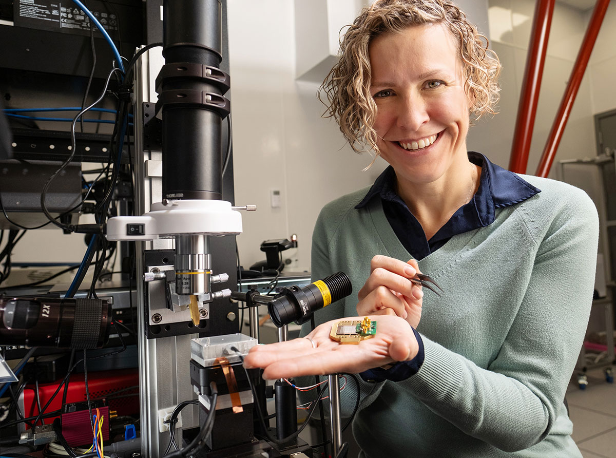
Photonic Inc. founder and chief quantum officer Stephanie Simmons, with one of the company’s quantum silicon chips. [Image: Photonic Inc.]
On 8 November, Photonic Inc., a quantum technology startup based in Vancouver, BC, Canada, announced that it had entered into a strategic collaboration with the multinational IT giant Microsoft Corp. Under the arrangement, the pair will develop a quantum-networking roadmap, and Microsoft will gain access to Photonic’s silicon-based quantum technology for Microsoft’s Azure cloud platform.
Separately, Photonic revealed that it had secured US$100 million in new venture funding from a consortium of investors including Microsoft and a variety of other capital partners. And the startup firm provided technical details about its envisioned quantum architecture, built around networks of silicon spin qubits connected with photonic links through spin–photon interfaces in silicon.
In a press release unveiling the new architecture, Photonic Inc.’s founder and chief quantum officer, Stephanie Simmons (featured this past July as one of OPN’s Entrepreneurs to Watch), laid out an ambitious timeline for the company. “We believe that—within five years, significantly sooner than the widely accepted timeframe—we will be the first quantum computing company to offer a scalable, distributed, and fault-tolerant solution.”
Betting on silicon T centers
Simmons founded Photonic in 2016 to commercialize the technology of spin–photon interfaces in silicon, a focus of her lab at Simon Fraser University, Canada. The company has since operated in stealth mode, developing the technology and building staff—which has now reached around 120 persons—and funding. In a mid-2023 interview with OPN, Simmons referred to Photonic as “the biggest quantum computing company that you’ve never heard of.”
Simmons has referred to Photonic as “the biggest quantum computing company that you’ve never heard of.”
The company’s approach rests on the quantum virtues of a specific type of radiation-damage center in silicon, known as T centers. These silicon “color centers” reportedly have long-lived quantum spins, enabling them to act as robust qubits. They also have well-behaved optical transitions in the telecom O-band, allowing them to talk with the outside world.
In a 2022 paper in Nature, a team led by Simmons revealed that it had found a way to integrate thousands of individually addressable T-center spin–photon “micropucks” in a silicon wafer and to optically read out the spin states. Since then, Photonic has reportedly developed ways to put a million such silicon qubits on a single chip.
From spin–photon qubits to quantum networks
Speaking with OPN in mid-2023, Simmons noted that Photonic “believe[s] that quantum networks and quantum computers will ultimately be the same technology.” In a new posting on the arXiv and a white paper released in early November, she has now detailed how the company’s core technology of silicon spin–photon qubits might be extended into an architecture that “offers a combined single technological platform for scalable fault-tolerant quantum computing and networking.”
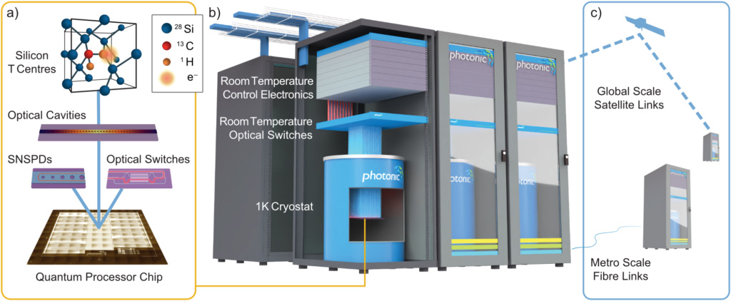
Photonic Inc.’s proposed “scalable quantum technology architecture” includes quantum chips hosting silicon T centers, cooled in a 1K cryostat, with optical cavities, photonic switches and single photon detectors handling the optical processing of quantum information from the T-center qubits. Optical I/O ports through optical fiber enable nonlocal connectivity and horizontal system scaling—and thus, according to Photonic, expansion of computing power and long-distance quantum networks. [Image: Photonic Inc.]
The architecture involves cryostatically cooled silicon quantum chips packed with T centers, linked through integrated photonics and fiber optics in a highly connected, wide-ranging network. One key feature, described in the arXiv posting, is the potential use of silicon T-center processors not only for quantum computing, but as the foundation for so-called quantum repeaters. Such repeaters—tricky memory components required for keeping delicate quantum information alive in messy, global terrestrial fiber networks—have been a long-standing things-to-do item holding back visions of a quantum internet.
According to Photonic, the architecture it has sketched out benefits from a variety of factors, including the maturity and ubiquity of silicon in modern computing infrastructure, the natural compatibility of silicon T centers with standard telecom wavelengths, and the high quality and quantity of input/output these color centers enable. The company also says that the architecture’s support for non-local connectivity—basically, enabling any quibt in the network to talk with any other qubit—opens the door to high-quality error-correcting techniques. In a blog post, Photonic’s CEO, Paul Terry, maintained that the architecture “allow[s] us to leverage the memory and computing capabilities of spins with the connectivity of photonics,” and “to scale our system horizontally and, thus, form the building blocks of a truly scalable, fault-tolerant system.”
Partnering with Microsoft
The recently announced collaborative arrangement with Microsoft will presumably offer Photonic an interesting testbed for the new architecture.
The recently announced collaborative arrangement with Microsoft will presumably offer Photonic an interesting testbed for the new architecture. In a post on the Microsoft Azure Quantum Blog, Dennis Tom, the general manager for the company’s Azure Quantum division, said the two companies shared a mission to “unlock the next stages in quantum networking and empower the quantum computing ecosystem.”
The collaborative project will focus particularly on distribution of quantum entanglement across long distances, using photons and Microsoft’s global cloud infrastructure. The companies plan to proceed in three stages.
The first stage, according to Tom, will be achieving entanglement between two separate quantum devices via fiber optic links. The second will be developing a “never-before demonstrated quantum repeater” for the required interim storage of quantum information. And the final stage will focus on making the quantum repeater reliable, fault tolerant and operational in Microsoft’s cloud infrastructure, enabling “the ability to create a full-scale, global quantum internet.”
New funding
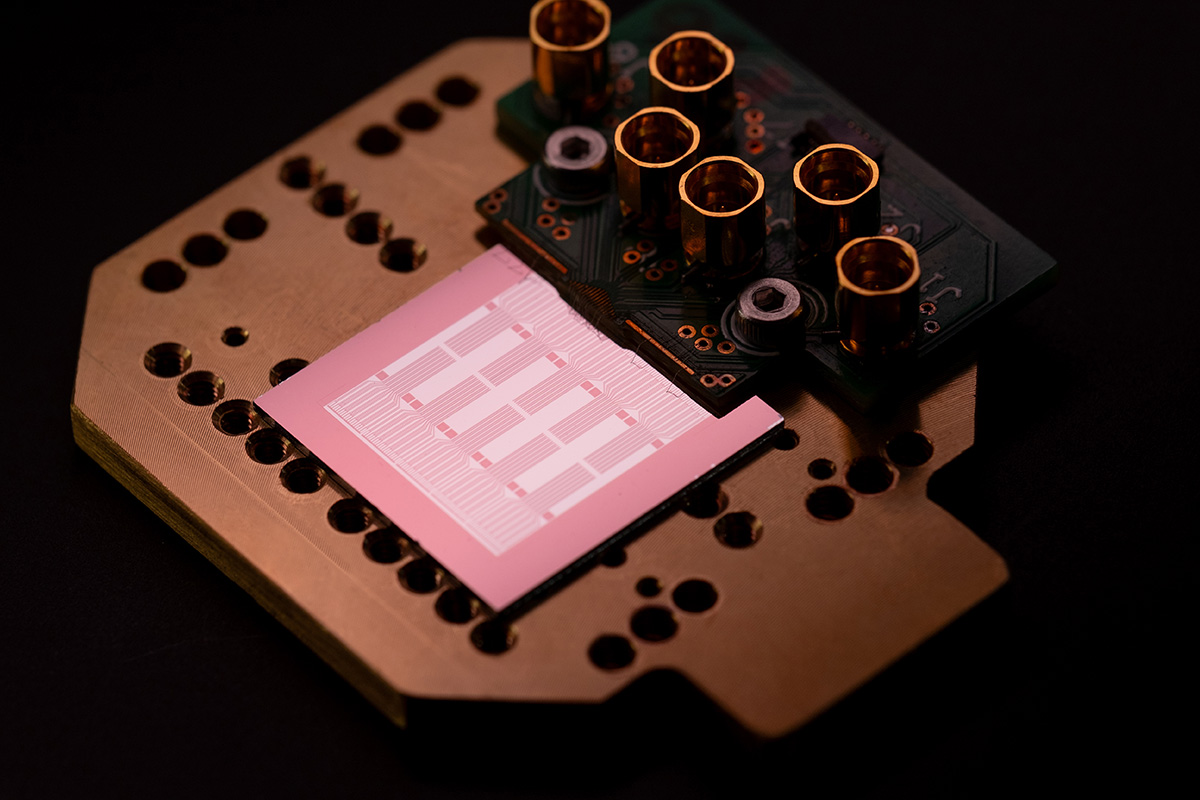
Photo of a Photonic Inc. chip. The company’s technology is built around spin–photon qubits in silicon. [Image: Photonic Inc.]
For Photonic, the recently announced US$100 million in new funding will help underwrite this ambitious roadmap. In addition to Microsoft, investors in the round included British Columbia Investment Management Corporation (BCI), the UK government’s National Security Strategic Investment Fund (NSSIF), Inovia Capital and Amadeus Capital Partners. The new tranche brings Photonic’s total funding to date to US$140 million.
Photonic believes its silicon-centric vision of quantum computing and networking has the potential for applicability both in areas such as global internet cybersecurity (through quantum encryption) and for scientific applications in climate modeling, materials science and drug development. While acknowledging that the company’s target of scalable, distributed, fault-tolerant quantum computing within five years is “audacious,” CEO Terry believes that the firm’s new architecture “is uniquely positioned to reduce the world’s time horizon to practical and useful quantum computing and quantum networking.”


