
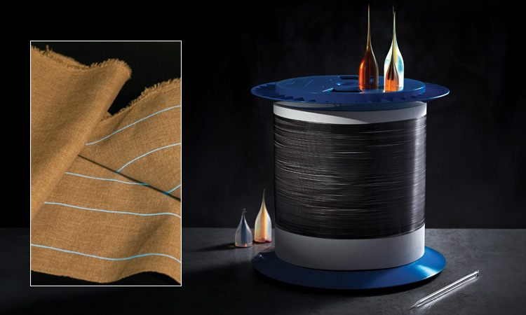
 A spool of thermally drawn semiconductor fiber and multiple preforms featuring the “preform-to-fiber” transition neck. Inset: A sample of wearable fiber fabric. [Z. Wang and L. Wei]
The global market for wearable devices is expected to grow steadily from US$54,125 million in 2024 to approximately US$149,692 million by 2032. This growth is driven by the rising demand for technologies that seamlessly integrate into daily life while enhancing connectivity, health monitoring and convenience. Consumers are drawn to wearable devices that offer comfort, compactness and multifunctionality. This pursuit of a smarter lifestyle has led to the emergence of new forms of smart devices, including smartwatches, fitness bands, smart glasses and even smart helmets. Moreover, traditional gadgets are evolving into new, flexible forms, such as foldable smartphones.
While wearable devices are primarily designed for areas where people typically wear accessories, like wrists, heads or eyes, functional clothing remains rare, largely due to challenges such as the high cost of development, technical complexities in embedding electronics seamlessly into fabrics, and consumer hesitance to adopt such innovations in daily wear.
Current wearable designs rely on rigid, planar components connected by flexible structures, so often require compromises in user comfort and device placement. In contrast, clothing made from woven fibers offers superior flexibility, lightweight comfort, breathability and mechanical durability—qualities ideal for wearable applications. Despite these advantages, clothing has largely remained limited to its traditional roles of physical coverage and aesthetic expression, and is yet to achieve significant evolution in terms of functionality.
 [Enlarge image]Integration of fiber devices in different application scenarios could seamlessly improve our daily lives. [Z. Wang and L. Wei]
A new era in wearables
Integrating functional fibers—particularly optical and optoelectronic fibers—into wearable technology could usher in a new era of smart clothing that maintains the comfort and versatility of traditional fabrics while serving as wearable devices.
Fiber-based wearable technology has the potential to reduce the weight of the technology users carry daily by replacing bulky components with lightweight, flexible materials.
Fiber-based wearable technology has the potential to reduce the weight of the technology users carry daily by replacing bulky components with lightweight, flexible materials that can seamlessly integrate into textiles. Separate devices, like smartwatches and smartphones, add extra load. Clothing embedded with multifunctional fibers would allow users to carry more technology, blending functionality with daily wear without increasing physical burden.
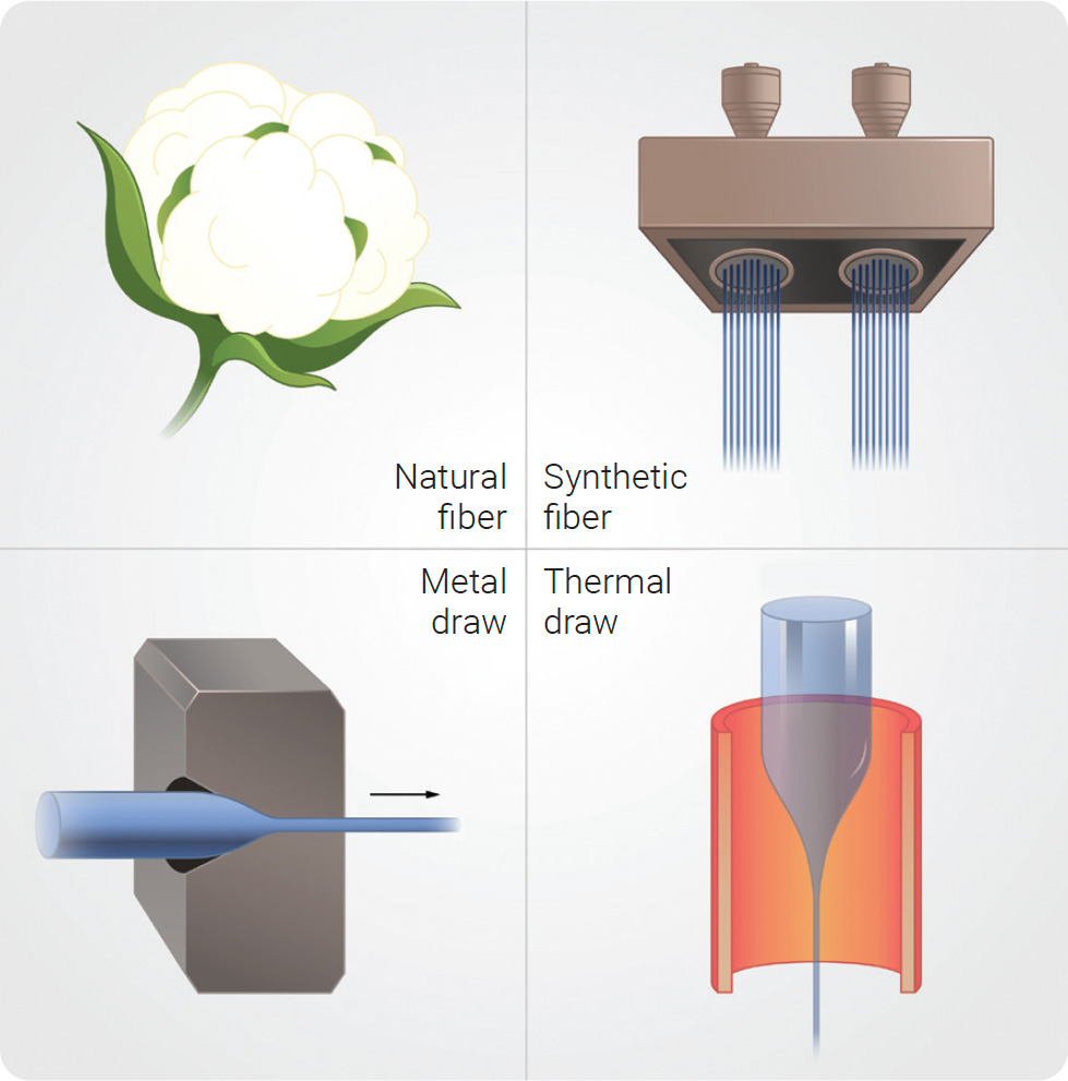 [Enlarge image]Historically, fibers have transformed industries, from natural textiles to synthetic fibers, metal wires and optical fibers, which revolutionized global communication. [Z. Wang and L. Wei]
Fibers, defined as collections of physical items with an aspect ratio (length to diameter) greater than 100, can consist of single materials or complex composites. They are ubiquitous and have historically transformed how we live: first, we learned to extract and utilize natural fibers; then the invention of synthetic fibers greatly expanded the range of available products; and, later on, the advent of optical fibers revolutionized communication and interconnected the globe. Today, another evolution—one that could redefine wearable devices—might be just around the corner. Fiber devices are also well-suited for integration into commercially popular wearable devices at present, which usually combine rigid and flexible components, such as smartwatches with rigid cases and flexible straps. Due to their lightweight nature and unique form factor—resembling jump wires—fiber devices can be embedded within the rigid parts, occupying minimal space, or serve as the flexible straps themselves. Connections between fibers and other components can be established through various methods, including wiring and soldering, conductive pastes, magnets, or pogo pin-like mechanisms. This ease of integration highlights the significant potential of functional fibers in advancing wearable devices.
To realize this transformation, fibers must integrate multiple materials into carefully designed structures. Fabrication methods typically involve a single or a blend of materials. However, achieving multi-material fibers with designed structures demands innovation in both fiber design and fabrication techniques. Integrating materials with distinct properties—such as waveguides and structural supports; metals, semiconductors and insulators; or crystals and amorphous materials—is essential for achieving functionality. Traditional material blending rarely results in a functional device. Instead, careful structural design combined with fabrication techniques that can handle multiple materials and are capable of forming specific structures are required to create working gadgets. However, direct adaptation of manufacturing processes designed for planar devices often encounter challenges. The unique characteristics of fibers, such as high curvature, small diameter, long length, and other features, impose specific constraints on fabrication.
From bulk to devices: Advances in fiber technology
Recent breakthroughs in fiber technology include integrating semiconductors and optoelectronic materials into fiber structures. Early innovations involved using glass fibers as waveguides for optical communications, a milestone pioneered by Nobel laureate Charles K. Kao during the 1960s. Shortly after, other materials, such as the semiconductor chalcogenide glass, were developed into fiber form for infrared applications. In the 2000s, Anna C. Peacock and John V. Badding developed a high-pressure deposition technique to produce crystalline semiconductor fibers. Around the same time, John Ballato and Ursula. J. Gibson advanced the molten-core method for fabricating crystalline semiconductor fibers. While the primary focus of these semiconductor fibers was optical waveguides, their potential expanded into other optoelectronic and electronic applications.
The scientific community has since explored this capacity through advances in fiber design and fabrication. For example, Xiaoming Tao innovated synthesis methods for fibrous materials and developed system-level integrations of fiber sensors as wearable devices, replicating the five human sensory functions. Meifang Zhu conceived the FIBER concept—Functional, Integrated, Brainy, Electronic and Responsive—aiming to revolutionize fiber structures and materials. Based on the thermal drawing technique initially used for fabricating glass optical fibers, Yoel Fink and his team at the Massachusetts Institute of Technology, USA, extended its scope by incorporating a diverse range of materials, enabling fibers with electronic and optoelectronic capabilities.
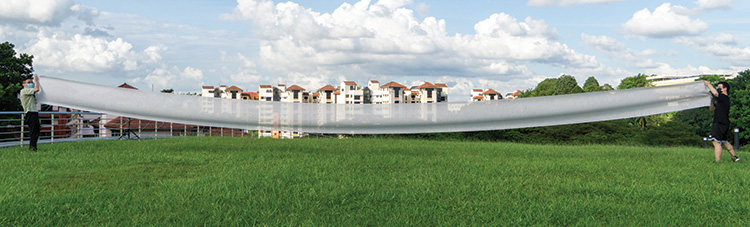 A large-scale functional fabric enabled by thermally drawn optoelectronic fibers. [Courtesy of B. He, S. Yuan and Z. Wang]
Fiber crossbars: Weaving functionality
Weaving is one of humanity’s oldest manufacturing techniques, and it continues to play a role in modern smart textiles by enabling scalability and enhancing the functionality of fiber-based materials. The interlacing of warp and weft yarns remains the most effective method of using fiber materials.
Fiber crossbars, the textile architecture created by weaving, have emerged as a basic building block for state-of-the-art smart wearables. A crossbar consists of two interlaced fibers that interact frequently, enabling the formation of functional devices at their crosspoints. Multiple fiber crossbars can be integrated into various textile structures, such as plain weaves or knits, to create large arrays with more advanced functionalities.
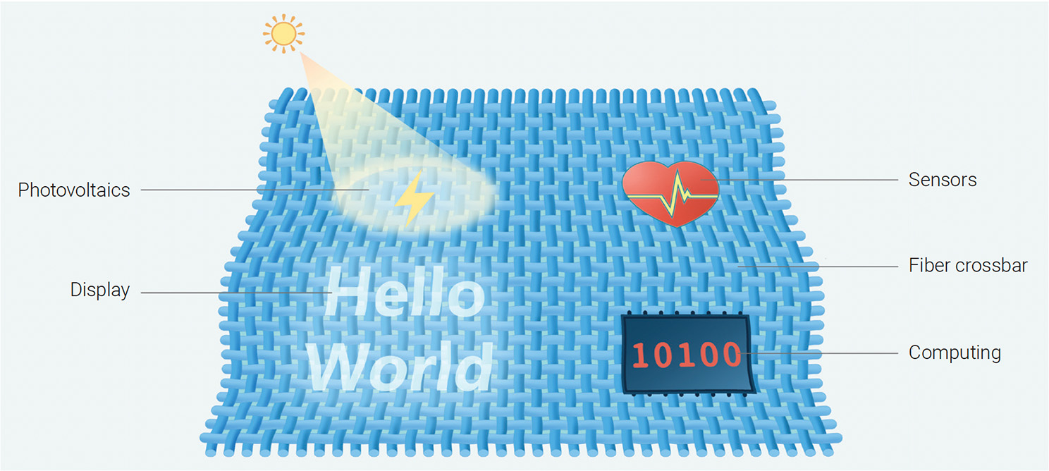 [Enlarge image]Fiber crossbars as the basic interlaced structure in fabrics for forming functional units. From energy harvesting and sensing to display and computing, various functionalities can be achieved from the weft touching the warp. [Z. Wang and L. Wei]
In a 2021 study, Huisheng Peng’s team at Fudan University, China, developed a 6-m-long, 25-cm-wide display textile containing 5×105 pixels. This wearable display was fabricated by weaving conductive weft fibers with luminescent warp fibers, creating micrometer-scale electroluminescent units at the weft–warp crosspoints. The researchers used ionic-liquid-doped polyurethane to prepare transparent conductive weft fibers via melt-spinning, together with ZnS phosphor-coated silver-plated conductive yarn to create display textiles that are flexible and breathable and withstand repeated machine-washing. Their display, combined with a power supply and a keyboard, formed an integrated textile that functions as a communication tool. Each press on the keyboard generates an input, which is processed by an external microcontroller programmed to output corresponding text. The text is then displayed on the display textile. This wearable optoelectronic textile is expected to form the next generation of communication tools.
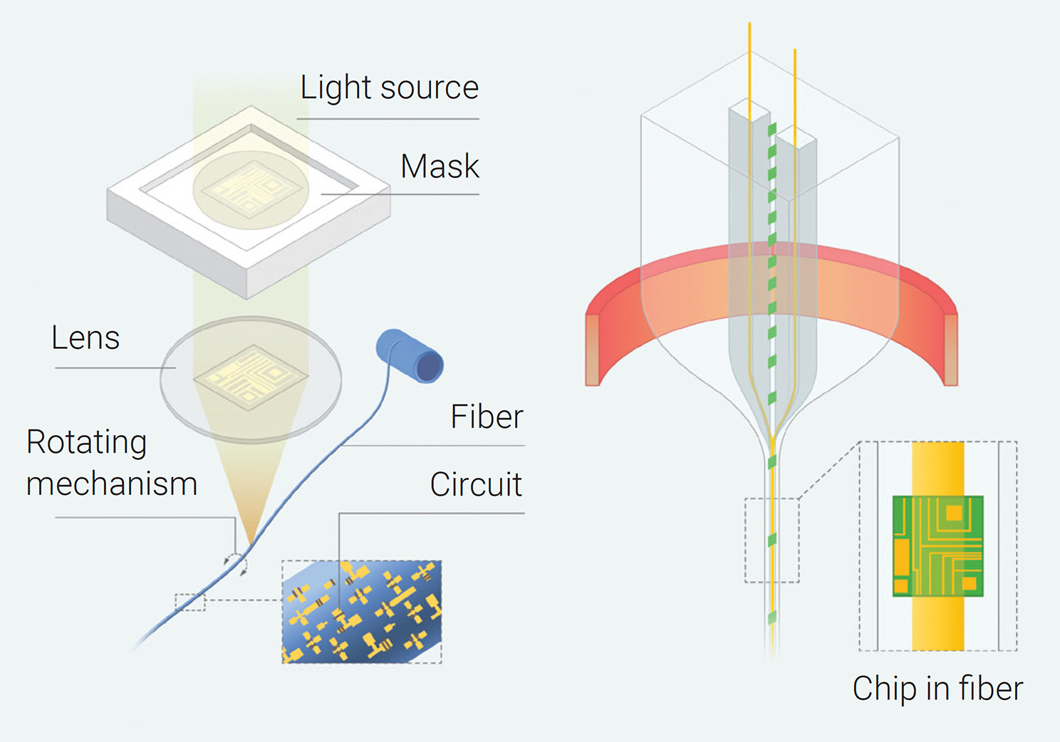 [Enlarge image]Left: Schematic showing how lithography may be adapted in fiber platforms to “write” circuits. Right: Schematic of using thermal drawing technology to combine planar chips with fibers. [Z. Wang and L. Wei]
Integrating chips in fiber form factors
Another approach to achieving optoelectronic fibers involves integrating planar-type chips into a fiber form factor. In a study, Tae-Wook Kim at Jeonbuk National University, Republic of Korea, and colleagues developed an electronic fiber platform enabling large-scale integration of planar-type devices on the surface of a 150-μm fiber. Using high-resolution maskless photolithography combined with a capillary tube-assisted coating method, the team fabricated chips consisting of field-effect transistors, inverters, ring oscillators, photodetectors, transducers and thermocouples onto the sides of the fiber substrate. This high-density integration of planar-type devices on a fiber enables multiple functionalities, including UV detection and switching electrical signals in a single transistor, symmetric input/output (I/O) behavior in the n-type inverter, oscillation characteristics of a five-stage ring oscillator, and thermal sensing. This approach served as a proof of concept for assembling multiple electronic systems on a single microfiber, paving the way for monolithic fiber devices.
In addition to forming devices on fiber surfaces, convergence thermal drawing is an alternative technique for fabricating monolithic fiber devices using commercial chips. Fink’s team developed this approach by combining scalable preform-to-fiber methods with commercial chips to create high-performance optoelectronic fibers. The process begins with placing discrete commercial chips inside a macroscopic preform designed with internal structures to accommodate the chips and later-fed metal wires. During the thermal drawing process, the metal wires approach the chips and eventually converge on their surface, making full contact and establishing electrical connections. This method enables simultaneous in situ electrical connectorization and device packaging, unlocking optical communication functionalities for fibers and textiles at unprecedented data rates, and integrating various alternative electronic devices into thermally drawn fibers.
Integrating commercial chips with fiber substrates enables high-performance devices but faces challenges such as low device density and complex lithography processes.
Fiber devices from all-fiber components
Integrating commercial chips with fiber substrates enables high-performance devices but faces challenges such as low device density and complex lithography processes, which limit the length of the device—an essential factor for fiber-shaped applications. Using all-fiber components presents a promising alternative. In particular, the thermal drawing technique holds significant potential for harnessing all-fiber components to create monolithic fiber devices. The first step is to prepare all the necessary materials—categorized as conducting, semiconducting and insulating based on their electrical properties—in a fiber form factor. Due to their excellent machinability, conductors, typically metals, can be pulled into fibers. For insulators, thermoplastics are well-suited for fiber formation thanks to their outstanding thermal processing characteristics. However, fabricating semiconductors—particularly crystalline semiconductors—into fibers remains challenging. While various crystal growth methods have been developed for producing semiconductor fibers, they yield far less material than wafer production, which benefits from slicing a grown ingot into multiple wafers. By contrast, the large aspect ratio of fibers results in a much smaller yield.
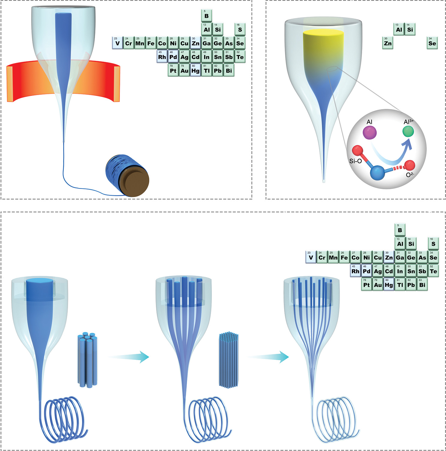 [Enlarge image]Schematics of fiber fabrication via the molten-core method. Top left: Elements reported (green) and elements potential (light blue) to be processed into fiber form factor; top right: elements reported to be processed via reactive draw; bottom: multi-core fiber fabrication via the stack-and-draw method. [Z. Wang and L. Wei]
The molten-core method, which leverages the high yield of the thermal drawing technique, has also been explored for producing glass-clad semiconductor core fibers at extended lengths. When modified to incorporate additional materials, the molten-core method creates new interfaces, particularly between the glass cladding and the semiconductor core. These interfaces contribute to more complex in-fiber stress distributions, potentially causing perturbations or fiber fractures. To address these challenges, a comprehensive mechanical study of each stage of fiber formation is essential for establishing a rational mechanical design, ensuring the production of ultralong, continuous, perturbation-free and fracture-free semiconductor fibers. Subsequently, a theoretical framework was developed to analyze the morphology and stress evolution across the three key stages of fiber formation in the molten core method—the viscous flow stage, the core crystallization stage and the cooling stage—enabling the fabrication of high-quality, continuous semiconductor fibers.
With conducting, semiconducting and insulating materials now accessible in a fiber form factor, the next step is to assemble them into functional devices. These materials have distinct thermal characteristics, making convergence thermal drawing a promising approach as all-fiber components form functional structures in situ during the draw. A proof of concept was demonstrated by constructing in-fiber back-to-back Schottky diodes by converging fed-in semiconductor and conductor fibers within an insulating preform. This process simultaneously achieves the formation of device configuration and packaging in a single step.
Leveraging its unique form factor and optoelectronic performance, this fiber offers photodetection at extended lengths and the ability to conform to curved surfaces where traditional rigid, discrete photodetectors cannot be applied. Additionally, their mechanical robustness enables them to be woven into large-scale functional fabrics while maintaining desirable properties such as conformability, washability and permeability. These optoelectronic fibers deliver performance comparable to commercial planar photodetectors and open up diverse applications, including in health care, robotics, wearable communications and assistive technologies.
Toward practical applications
The commercialization of fiber devices is at an exciting yet formative stage. While current fabrication meets the scale of production, further advancements are needed to diversify the processable types of fiber devices and their functionalities to fulfill potential customers’ needs for widespread commercialization. Niche applications, such as illuminated fibers in stage costumes or fiber sensors integrated into wristbands or headbands to monitor heart rate, blood oxygenation and other metrics, have already demonstrated the potential of this technology.
Numerous proof-of-concept fiber devices have been successfully developed in labs, most of which focus on sensing, displaying, actuating and energy storage. However, fiber devices related to data processing have been less frequently reported. Currently, planar-type interface boards are still required for data processing and managing I/O within fabric systems. Developing in-fiber high-throughput I/O interfaces and computing fibers is essential to realizing a fully integrated fiber-based system.
High-throughput I/O is crucial for unlocking applications requiring rapid data exchange and complex functionalities. Commercial I/O cables typically take the form of flat ribbons with connected fibers, allowing for convenient installation in planar-type devices, such as behind the display panels of monitors. However, this flat ribbon form factor is not suitable for all-fiber systems. Novel approaches, such as three-dimensional connectors or fiber-to-fiber communication protocols, are required to enable seamless integration and optimize volume utilization. In addition to electrical I/O interfaces, optical communication technologies present a promising solution for establishing high-throughput I/O in fiber devices, either being integrated within individual fibers or using the entire fiber as an optical waveguide. Overall, achieving high-throughput I/O in fiber devices requires interdisciplinary efforts combining materials science, optics and electronics engineering to create innovative solutions that meet the demands of next-generation fiber-based wearables.
Besides I/O interfaces, computing fibers with integrated computational capabilities are crucial for developing a full-fiber system akin to the role of a CPU in a traditional computer. Achieving this requires the integration of semiconducting, conducting and insulating materials into complex architectures within the fiber. Unlike systems that rely on transmitting data to external microcontrollers, computing fibers can process data locally from fiber sensors and others. This reduces latency and enables real-time applications in areas such as health monitoring, human–machine interfaces and adaptive clothing. Additionally, quantum computing fibers hold significant promise, leveraging the advantages of fiber form factors in optics to address the unmet need for high-performance computation in fiber-based systems.
Overcoming challenges
Although fiber devices have found practical applications in niche markets, broader commercialization requires overcoming several challenges, with the expansion of material scope being a primary concern. Material availability for fiber device fabrication must align with the specific functional requirements, target applications and user preferences. This involves not only identifying materials with the necessary properties but also adapting them to the fiber form factor.
The core challenge lies in broadening the range of materials that can be processed into fiber form or integrated into fiber structures while maintaining exceptional performance. This includes developing novel materials and modifying existing ones—such as metals, semiconductors, polymers and composites—to meet the unique demands of fiber-based applications. For example, the fabrication of silicon fibers provides the basic units for realizing fiber-shaped chips. Manufacturing other semiconductors, such as gallium nitride and silicon carbide, into fiber form factors is essential for creating fiber-shaped power devices. Other examples of materials being processed into fiber form for novel fiber devices include perovskites, MXenes and superconductors. These new functional fibers can be used independently or combined with commercial non-functional fibers, such as cotton or nylon, in mixed weaves or twisted threads to share mechanical loads.
The ability to engineer and process a wider scope of materials in fiber form will be key to advancing smart fiber technologies and unlocking their potential.
Additionally, these materials must be compatible with scalable fabrication techniques to ensure efficient production. Ultimately, the ability to engineer and process a wider scope of materials in fiber form will be key to advancing smart fiber technologies and unlocking their potential in health care, wearable electronics and beyond.
Another critical factor for the widespread application of fiber devices is their dimension. Commercial non-functional fibers used in clothing are typically thinner than a dtex (ultrafine fiber)—approximately 10 μm or thinner. In contrast, current fiber devices, particularly monolithic ones, often have significantly larger diameters. Fabricating thinner fiber devices, particularly with diameters under 10 dtex, is essential for advancing fibers’ application in wearable technologies. A fiber of this dimension strikes an optimal balance between flexibility, lightweight properties and mechanical robustness, making it ideal for integration into fabrics without sacrificing comfort or breathability.
Additionally, thinner fibers improve functional units’ spatial resolution and density within fabric-based devices. For example, in applications like wearable displays, sensors or energy storage, finer fibers enable a higher density of devices per unit area, enhancing functionality and performance while maintaining a natural feel. From a practical perspective, thinner fibers are more compatible with traditional textile manufacturing methods such as weaving and knitting, enabling seamless integration into everyday clothing. This compatibility is vital for the development of advanced fiber devices that are indistinguishable from conventional fabrics, promoting user adoption and paving the way for next-generation wearables.
Zhixun Wang and Wei Lei are with Nanyang Technological University, Singapore.
References and Resources
-
Credence Research. Wearable Devices Market. Report ID:42327. Retrieved from www.credenceresearch.com.
-
X. Shi et al., “Large-area display textiles integrated with functional systems,” Nature 591, 240 (2021).
-
S. Hwang et al., “Integration of multiple electronic components on a microfibre towards an emerging electronic textile platform,” Nat. Commun. 13, 3173 (2022).
-
M. Rein et al., “Diode fibres for fabric-based optical communications,” Nature 560, 214 (2018).
-
Z. Wang et al., “High-quality semiconductor fibres via mechanical design,” Nature 626, 72 (2024).
