
 [Getty Images]
The release of Open AI’s generative-AI chatbot, ChatGPT, in November 2022 was the technology shot heard ‘round the world, opening what seemed to be new vistas of productivity and potential across the business landscape. And although much of the initial public hype has since been tempered, the continued rapid growth of AI-capable infrastructure in data centers, and of AI-enabled thinking in the product lab, is creating intriguing opportunities for the optics and photonics industry.
For a taste of how all of this is unfolding, OPN recently spoke with representatives from six companies looking at pieces of this marketplace. While the resulting snapshots tell only a small part of a very big story, they do hint at how generative AI’s data needs have catalyzed a ferment of activity in silicon photonics—and also at AI’s broader impacts on how optics firms think about their other product offerings.
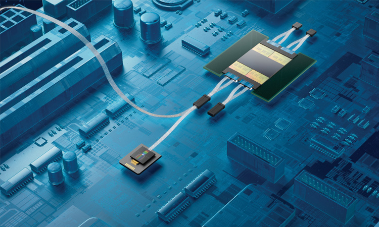 TeraPHY in-package optical I/O chiplet and SuperNova multiwavelength light source. [Ayar Labs]
Chiplet time
For silicon photonics, much of the action in serving these markets lies in solving AI’s “data bottleneck.” That’s shorthand for the increases in latency and energy consumption that occur as AI-enabling CPUs, GPUs and application-specific integrated circuits (ASICs) suck in data at an ever more furious pace from off-package computational resources—memory modules, for example, or other ASICs—across copper interconnects.
Numerous companies are converging on a similar solution to that quandary: silicon photonic “chiplets” that push the conversion between the electrical and optical domains as close to the GPU as possible, allowing connectivity across distributed computing resources to stay encoded as fast, energy-efficient light in optical fiber. One company that has plied these waters for nine years is Silicon Valley–based Ayar Labs. Ayar was born in May 2015 out of work (later reported in Nature) from labs at the University of California, Berkeley, the University of Colorado and the Massachusetts Institute of Technology (MIT), USA, demonstrating what Ayar now calls “the world’s first processor to communicate using light.”
Terry Thorn—who joined the firm as vice president of commercial operations three years ago, after 24 years in various roles at the semiconductor giant Intel Corp.—told OPN that Ayar’s work focuses on problems in the “scale-up” domain inside compute systems. That’s the domain that involves shunting data between compute chips, be they a CPU and GPU, two GPUs or a GPU and a distributed memory host. (It contrasts with the “scale-out” domain involving data transmission out of the server rack to other servers, and typically the sweet spot for traditional pluggable transceivers.)
In the scale-up domain, when a myriad of traditional copper interconnects is replaced by optical links carried in fiber, “you benefit a lot, obviously, from reduced latency and reduced energy,” according to Thorn. “And the closer we can put our connection to a compute chip, the more we’re able to take advantage of that efficiency benefit.” It’s in the scale-up domain, he said, that Ayar sees “the greatest immediate benefit, and where we have the greatest urgency and interest from our customers.”
Ayar’s vehicle for addressing that interest is a chiplet with the slightly whimsical name TeraPHY (pronounced “terrify”). The chiplet is designed to be integrated in-package with the electronic GPU or CPU, allowing electrical data to be immediately encoded (via systems of microring resonators) into optical data and sent out to other, similarly equipped compute resources on ribbons of optical fiber.
At OFC 2023, Thorn said, Ayar showed a “very stable demonstration” of its chiplets running “in live silicon” in a 4-Tbps bidirectional connection (that is, 2-Tbps in each direction) that used an energy-stingy 5 picojoules (pJ) per bit. The high data throughput was enabled by wavelength-division multiplexing in eight fiber connections to the chiplet, each hosting eight wavelengths of light carrying data at 32 Gbps apiece. Eight months later, in November 2023, Ayar demonstrated a similar system packaged with Intel field-programmable gate arrays (FPGAs) “running live, for days on end,” according to Thorn.
The other key component in these demos, and in Ayar’s offering, is its off-chip light source, trade-named SuperNova, that plugs into the chiplet. While the version used in the OFC 2023 demonstration supported eight wavelengths, one year later, at OFC 2024, Ayar unveiled an upgraded 16-wavelength SuperNova that the company says can “drive 256 optical carriers for 16 Tbps of bidirectional bandwidth”—a level of zip that Thorn thinks the company will demonstrate publicly in the next several years. In addition to changing the number of wavelengths, Thorn said, Ayar can use “a number of other levers” to push throughput, including adding fiber ports to the chip and boosting the data modulation per wavelength from the current 32 Gbps.
“One of the bigger challenges we all face is the momentum that has been built around electrical and copper,” said Ayar Labs’ Terry Thorn.
Thorn sees Ayar’s public demonstrations of steadily increasing capabilities in “live silicon” as an advantage for the firm as it plays in an increasingly competitive interconnects marketplace. Another plus, he said, is the company’s embrace of standards such as the emerging Universal Chiplet Interconnect Express (UCIe) framework for the electrical interface of its chiplet. Further, he noted that Ayar has engaged in a wide variety of partnerships to propel use cases forward, with firms including the GPU maker NVIDIA, the Swedish telecom firm Ericsson, Lockheed, Lumentum, the US Department of Defense, and even companies, like Intel Corp., that are working on their own silicon photonics solutions for AI.
In thinking about competition in this market, however, Thorn is philosophical. While recognizing that other players are also looking to take silicon photonics into solving AI’s bandwidth challenges, he believes the overall effort to wean customers off of conventional electrical interconnects will benefit all competitors in this space. “One of the bigger challenges we all face is the momentum that has been built around electrical and copper,” Thorn said. “If someone changes that mindset, and we can start a different flywheel around optics and silicon photonics, that helps lift all the boats.”
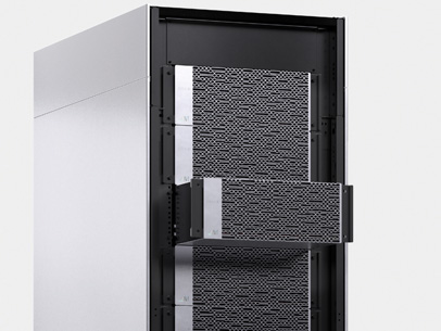 Lightmatter rack with one blade out. [Lightmatter]
Interconnects and AI accelerators
Another young company, Lightmatter, based in Mountain View, CA, USA, is advancing a broader vision of photonics for AI, embracing both optical interconnects for handling AI data and an accelerator chip to speed the actual calculations of computational neural networks. If funding progress is any guide, the vision seems to have resonated among investors: Lightmatter’s most recent round of Series C financing, in December 2023, pushed the firm’s total valuation to US$1.2 billion—putting it firmly in “unicorn” territory.
It’s been a heady journey for Lightmatter, founded only in late 2017 by Nicholas Harris, Darius Bunandar and Thomas Graham as they completed their graduate studies at MIT. Harris and Bunandar were working on silicon photonics processors for quantum computing when the sudden explosion of interest in machine learning inspired them to use these programmable platforms for AI applications instead. Graham, an MBA student, joined on the finance side.
Lightmatter says it’s “blurring the line between scale-up and scale-out networks,” and is animated in particular by the mission of reducing AI’s environmental impact.
Lightmatter says it’s “blurring the line between scale-up and scale-out networks,” and is animated in particular by the mission of reducing AI’s environmental impact. “The biggest question,” Bunandar, now Lightmatter’s chief scientist, told OPN, “is, how do we power [AI]? How do we offer faster and more efficient compute for the hyperscalers who are going to deploy and train these models today? … I think everybody can agree that the amount of energy that is required to host and train these algorithms is quite immense.”
An insatiable appetite for energy
The computing power required to run AI, especially generative AI, is much higher than that required by typical computer programs—for instance, a ChatGPT query requires on average 10 times as much electricity to process as running a Google search.
As of May 2024, data centers accounted for 1% to 1.5% of the world’s total electricity use, but this is projected to double by the end of the decade because of AI—along with carbon dioxide emissions from data centers. Google, for example, attributes its 50% increase in emissions since 2019 to energy demands for AI. The power needed to sustain the technology’s rapid growth is nearly doubling every 100 days. As demand continues to grow, optics and photonics firms are following different paths to solve the energy-scaling problem.
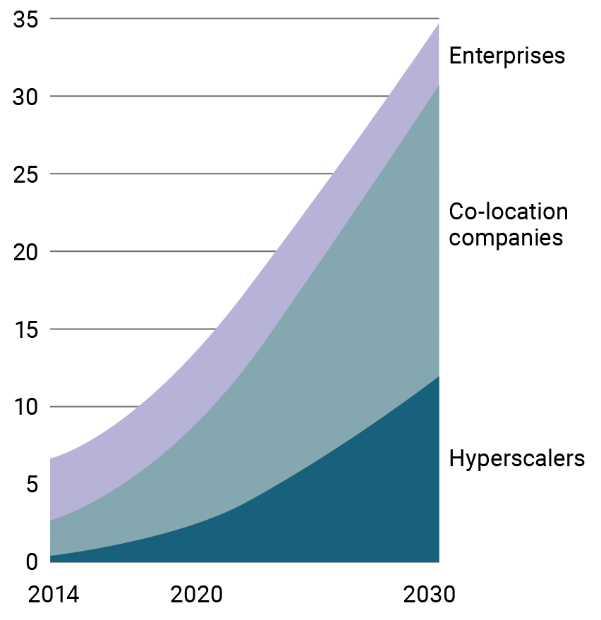 [Enlarge image]Data center power consumption in gigawatts, by providers/enterprises. [Data from McKinsey & Co., “Investing in the rising data center economy” (2023)]
Current chip technology, Lightmatter claims, has reached the limits of its ability to scale with AI’s burgeoning demands. The company’s solution is a full-stack suite of three technologies: Passage, a wafer-scale programmable photonic interconnect; Envise, a photonic AI accelerator chip; and Idiom, a software layer.
Passage integrates transistors and photonics, a combination that, according to Lightmatter, allows 40 waveguides to fit in the space of a single optical fiber. This reduces packaging complexity and cost, the company argues, while increasing performance. Since the photonic interconnect is built in, it removes the need for driving long wire traces between chips and optical transceivers. Lightmatter maintains that its “dramatic interconnect density improvement” provides over 10 times more I/O bandwidth than existing chip-to-chip interconnects and could drive greater than 100 times more bandwidth in five years.
“When we’re looking at training and deploying these generative-AI algorithms, more than 80% of the power is actually spent on data and memory movement,” Bunandar said. “We believe that Passage can play an important role in the market given that it can save the amount of power that is spent for memory-to-compute as well as compute-to-compute communication.”
Lightmatter refers to Envise, which Bunandar said has several pilot customers, as “the world’s first photonic computing platform.” A general-purpose machine-learning accelerator, it combines photonics, electronics and novel algorithms into a single module to tailor computing platforms for AI. While Passage aims to improve how chips communicate, Envise takes on how they calculate. In an interview with OPN in 2021 (optica-opn.org/news/0621-lightmatter), Harris compared a then state-of-the-art chip from NVIDIA, which drew 450 W of power, to Lightmatter’s, which used only 80 W, to highlight the increased efficiency, in line with the company’s mission of decreasing AI’s environmental impact. (It’s unclear, though, if the two products serve the same function.)
Together, Lightmatter says, its slate of products is poised to take on the growing compute demand stoked by the booming AI industry. “We believe that a new compute paradigm is required to support the current AI and next AI revolutions,” Bunandar said. “So we’re answering that call with the photonic technologies that we’re introducing ... We’re revolutionizing the way chips calculate and communicate.”
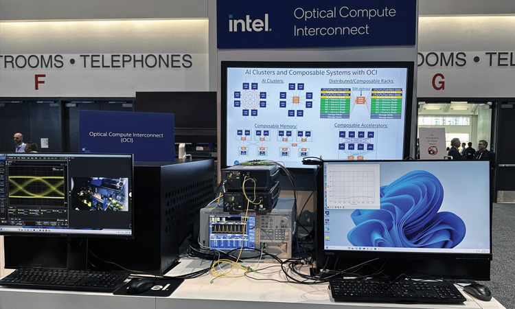 Intel demonstrated the OCI chiplet in its booth at OFC 2024. [Intel]
Chipmaker forays
Even as startup and early-stage firms have lunged forward to grasp the opportunities in AI, more-established firms in the semiconductor and networking businesses have hardly been standing still.
At OFC in March 2024, for example, the semiconductor giant Intel Corp. unveiled its own optical compute interconnect (OCI) chiplet, the capabilities of which it expanded on in a big press reveal in June (see optica-opn.org/news/0624-intel). The chiplet combines two copackaged systems—a photonic integrated circuit (PIC) embedding waveguides, amplifiers and dense wavelength-division multiplexing lasers, and an electronic integrated circuit with control circuitry and drivers. The result, according to Thomas Liljeberg, senior director of product management and strategy at Intel’s Integrated Photonics Solutions Group, is a “compact, fully self-contained I/O system” that “connects to the I/O port on your CPU or GPU, converts [the electrical signal] into an optical signal that can travel over fiber, and is converted back on the other end.”
 [Enlarge image][Celestial AI]
An active playground
Here’s a random sample of some of the many other firms attempting to carve out niches in the AI data space.
Celestial AI. The company’s offering is built around a “Photonic Fabric” that keeps data encoded as light not only to the edge of the GPU, but all the way to the “point of compute”—the precise point on the computer die where the number-crunching is taking place. The novelty of the concept has attracted substantial funding, as well as exploratory partnerships with what Celestial calls “some of the leading hyperscalers” as it works to build a “Photonic Fabric ecosystem.” [optica-opn.org/news/0524-fabric]
POET Technologies. The Toronto-based integrated-photonics firm is stressing its “Optical Interposer,” which POET calls “the first-ever wafer-level integration of electronics and photonics into a single device,” as a CMOS-compatible platform technology that can be used as a building block for co-packaged optics targeting AI applications at the transceiver and on-board levels.
Ranovus. Another Canada-headquartered firm, Ranovus, is specifically targeting optical interconnects in data centers through its Odin single-chip optical engine, which combines silicon photonics PICs with off-chip quantum dot lasers for AI/ML workloads. At OFC 2024, the firm announced that it was working with the Taiwan-based fabless semiconductor company MediaTek on “a 6.4-Tbps co-packaged optics solution” with “4-pJ/bit energy efficiency, including the laser.”
Quintessent. The California-based startup Quintessent has targeted laser sources as the “weakest link” for AI scalability, and hopes to strengthen that link through its own silicon photonics technology incorporating quantum dots and multiwavelength comb lasers. The company announced a US$11.5 million seed round earlier this year. [optica-opn.org/news/0624-quint]
In the OFC 2024 demo, Intel showed off a 4-Tbps bidirectional connection between CPUs through eight fiber pairs (with eight wavelengths per fiber), with an overall power efficiency of 5 pJ/bit. “You can think of it as 4-Tbps connectivity in a 10-W envelope, so it’s very, very efficient,” Liljeberg said. And he added that the firm sees “at least five or six generations of doubling-up on bandwidth with the same core technology,” through expedients such as increasing the number of wavelengths per fiber, the line rate per wavelength, and the number of fibers physically attached to the chiplet. Those multiple scaling knobs, Liljeberg maintained, give the firm “confidence that we’re heading down a healthy path” that can support future AI data transmission needs.
Intel—which has partnered in the past in demonstrations with companies like Ayar Labs—is well aware that it’s not the only player in the I/O market for AI. But the firm believes it has a number of advantages in the chiplet space. One is its ability to integrate reliable, indium phosphide–based lasers directly onto its silicon chips at scale—demonstrated, the firm points out, in the “over 32 million on-chip lasers” it’s shipped for the pluggable-transceivers market. Integrated lasers, Liljeberg noted to OPN, make sense in large part because they dramatically cut the coupling losses experienced by external lasers, a big plus “in a use case where the goal is the absolute best power efficiency.”
More broadly, Intel believes expertise in integration, at multiple scales, will be a key to winning in the AI-driven marketplace. Here, the company stresses the “more than around 2,000 components” integrated onto the PIC layer of its OCI chiplet; the company’s expertise in packaging and in constructing “complex die stacks” to bring the PIC together with the EIC into a single subsystem; and its abilities in integrating that subsystem into the compute platform. “You need to bring to bear all these disciplines and all these capabilities along the value chain,” Liljeberg said.
The foundry side
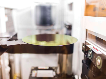
Semiconductor foundries, too, are in the game. For example, GlobalFoundries (GF), the company formed in 2009 from the spinoff of AMD’s manufacturing operations, is focusing on its silicon photonics platform, GF Fotonix, as a solution for building AI-friendly photonic interconnects.
 Wafer production at GlobalFoundries. [GlobalFoundries]
Anthony Yu, GF’s vice president of silicon photonics product management, came to the firm nine years ago and has been building its silicon photonics operation since 2017. GF’s early efforts focused on waveguide integration and monolithic integration of multiple electronic and optical elements, mainly for the pluggable-transceivers market. GF Fotonix, initially unveiled in 2022, is actually the third-generation offering—and, Yu told OPN, “kind of the sweet spot of what we have in AI.”
GF Fotonix is a 300-mm monolithic silicon technology platform, enabling copackaged optics and supporting 200 Gbps per wavelength in the C, L and O bands. It thus allows integration of a variety of optical elements such as modulators, couplers and multiplexers with CMOS-based electrical elements on a single die. GF claims that its integrated approach has enabled “the industry’s highest data rate per fiber.” And Yu stressed that GF currently has “the only 300-mm monolithic technology in production” in silicon photonics.
As a foundry, GF is a “platform play,” and in fact has partnered both with high-profile startups in photonic AI processing, including Lightmatter and Ayar Labs, and with much larger players with stakes in data centers and AI, such as NVIDIA and Cisco Systems. “We pick our partners carefully,” Yu said. In particular, GF looks for “startups we can collaborate with” strategically, and that can drive both GF’s learning in the AI sphere and, over time, the volume of its foundry business as the startups gain traction.
Among foundries, GF has pushed forward early in silicon photonics. But it’s not alone. In April 2024, for example, Taiwan’s TSMC, the world’s largest independent foundry, unveiled its own silicon photonics roadmap. Yu thinks such competition is good for the industry—“it provides choice,” he told OPN, “and sharpens us up.” GF, too, continues to invest heavily in silicon photonics, and will soon release a fourth-generation monolithic platform that should enable 400 Gbps per wavelength. Yu believes GF’s head start gives it an advantage in providing the low cost and manufacturability at scale that customers are now demanding.
As someone who’s worked for years to build up GF’s silicon photonics operation, Yu strongly senses that the advent of generative AI and the challenges of data bottlenecks and energy efficiency may finally drive the technology forward. “The need for photonics is now,” he said. “I think the moment is real. And that’s why we are completely committed to it.”
The potential of integrated photonics was illustrated by Nokia’s late-June announcement that it would acquire optical networking and PIC firm Infinera for the tidy sum of US$2.3 billion.
The network angle
Within the traditional optical-networking business, the potential of integrated photonics was illustrated by Nokia’s late-June announcement that it would acquire California-based optical-networking and PIC firm Infinera for the tidy sum of US$2.3 billion. Industry observers have noted how the purchase gives Nokia an entry into Infinera’s product lines in the data center interconnect (DCI) market and pluggable coherent optics. But even before the acquisition announcement, Tim Doiron, Infinera’s vice president of marketing, told OPN in an unrelated interview that the tremendous increase in traffic spurred in part by AI workloads—as well as opportunities that AI offers to improve customer service and experience—had prompted the company to think differently about its product offerings and internal processes.
 Infinera’s optical semiconductor fab in Sunnyvale, CA, USA, where it manufactures indium-phosphide-based PICs. [Infinera]
As one tangible result, Infinera has turned its gaze into the data center itself—a break from its historical focus on traffic between data centers. The company cited analysts at Cignal AI who projected that market demand for intra-data-center interconnect technology will grow nearly tenfold over the next four years, driven in large part by AI workloads. A company blog post also notes that GPU clusters for generative AI are scaling by a factor of 10 every three years.
In an effort to meet that staggering demand, in March 2024 Infinera launched ICE-D, a new line of high-speed intra-data center optics based on monolithic indium phosphide PIC technology. Infinera touts the “unique capabilities” of its optical semiconductor fab, as well as the advantages of indium phosphide for intra-data-center interconnects, including low loss and low power requirements. The company says that ICE-D components have demonstrated a reduction in power per bit—an important consideration in the context of power-hungry AI applications—by as much as 75%, while increasing connectivity speed, which is also a key factor in the AI landscape.
In a press release announcing the acquisition, Nokia specifically called out the ICE-D product line as a strategic benefit, as it is “particularly suited to AI workloads, which can become a very attractive long-term growth opportunity.” Infinera CEO David Heard also gave a nod to this new variety in products when the Nokia deal was announced. “We believe Nokia is an excellent partner,” he said, “and together we will have greater scale and deeper resources to set the pace of innovation and address rapidly changing customer needs at a time when optics are more important than ever—across telecom networks, inter-data-center applications, and now inside the data center.”
As Heard suggested, the boom in traffic from AI and machine-learning workloads is being felt between data centers as well, further driving Infinera’s core DCI business. As the capacity demands continue to rise, Infinera is looking to expand the usable spectrum to help network operators manage the need for bandwidth. According to Doiron, the company thinks that the time is right to expand the C band from its current 4.8 THz to 6.1 THz of transmission space, into the so-called Super-C band. “The economics and the performance are there to make that happen,” said Doiron, “to give you an additional 27% capacity expansion on the existing fiber that you currently have, without having to plow more fiber.”
The capabilities offered by AI have also inspired the company to reflect on its own processes. “When we look at AI, we see two aspects. One is additional drivers for bandwidth demand in the network,” explains Doiron. “But also, it’s an opportunity for us to look at our own business, and look at how we supply solutions to our customers, and how we can help our customers.” One such application is network health prediction, which could leverage AI to anticipate network issues and preemptively respond. There are also potential uses in customer service and for planning and executing marketing campaigns.
“While it’s early days, we’re going to continue to enhance and refine AI. We’re going to solve increasingly complex problems,” said Doiron. “And I really think AI has the power to transform the reliability, the resiliency, the anticipatory nature of our networks, and really turbocharge in many ways the efficiency of what we do and how fast we can go. It’s a great time to be working in an innovation that matters.”
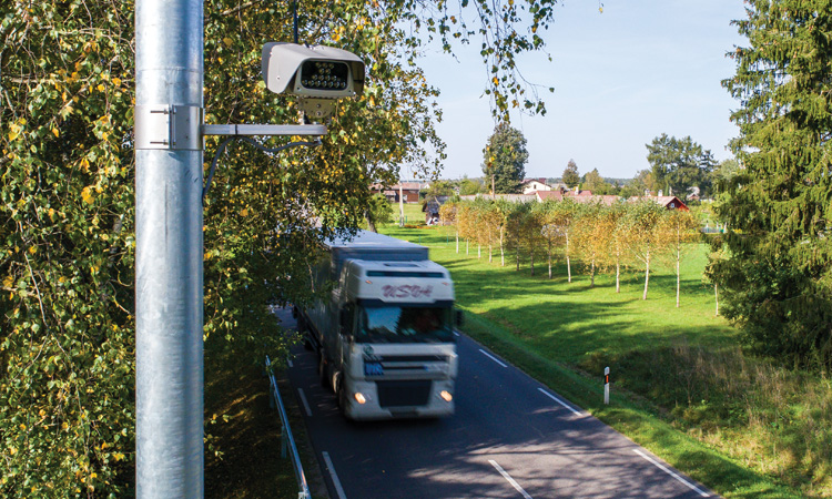 Jenoptik’s VECTOR cameras provide AI-enabled automatic license plate recognition solutions. [Jenoptik]
AI as a business optimizer
Infinera’s use of AI not only as a new business area but to improve existing operations is not a one-off, but a trend throughout the photonics industry. To get a read on this aspect of AI’s impact, we spoke with Germany-based Jenoptik to learn about how it is incorporating AI into current products and processes. With a corporate lineage dating back to the late-19th-century research partnership of Carl Zeiss, Ernst Abbe and Otto Schott, the global integrated-photonics firm has experience capitalizing on technological developments—and the growth of AI has been no exception.
“AI is really not a new topic for us … It has been used for many years within our optics and for our customers,” explained Adrian König, Jenoptik’s director of digital transformation and innovation. “Strategically, AI and machine learning have enabled us to enhance our existing product suite and innovate new offerings for our customers. Incorporating AI-driven analytics into our photonics products allows us to deliver more precise and reliable solutions for our customers. Or in the field of image processing—which is really a big deal for us in terms of AI—we have changed the way our customers are getting the information they need.”
According to Subhasis Pradhan, Jenoptik’s program manager for corporate innovation, the company started incorporating AI to improve its offerings in 2017, well before the explosion in attention spurred by the November 2022 launch of ChatGPT. The 2017 project was for the automotive industry, and involved applying a neural network to image processing to inspect screw heads for defects. High-resolution camera systems are combined with neural networks trained on large datasets of error-free components. They can then autonomously and accurately recognize whether production parts meet the defined quality requirements.
“Strategically, AI and machine learning have enabled us to enhance our existing product suite and innovate new offerings for our customers,” explained Jenoptik’s Adrian König.
This metrology application set some of the tone for Jenoptik’s subsequent use of AI in other segments. The company emphasizes finding a use case for delivering customer value ahead of innovation for its own sake. As Pradhan noted, “We saw the value of AI or machine learning, but it’s more important to bring the business opportunity together with the technology opportunity.” König expanded on the observation: “At the end, the problem itself isn’t the center of our focus. It’s how we want to solve a problem for our customer.”
One of the company’s three divisions, Smart Mobility, has seen particularly significant benefits from the integration of AI. This group has deployed AI-enabled automatic license plate recognition (ALPR) for civil security and law enforcement, as well as an AI-enabled toll collection system. These systems pair Jenoptik’s VECTOR2 ALPR cameras, which automatically capture vehicle license plates, with deep-learning software that accesses an existing portfolio of images to increase capture rates and more successfully read complete plates, even in challenging environments.
Another of the many companies taking a holistic approach to AI is worldwide laser and machine tool giant Trumpf , which has been outspoken about its plan to integrate AI into all facets of its operation. At a press conference in April, Trumpf Chief Technology Officer Berthold Schmidt said, “In five years’ time, we want to be the leading user and leading provider of AI solutions in our industry. By then, there should no longer be a job at Trumpf that does not have some connection to AI.” The company currently offers AI-enabled solutions for sorting cut components or improving assembly design in machine tools, and process control in laser technology. In mid-July, Trumpf announced a partnership with ML startup SiMa.ai to equip laser systems with SiMa’s AI chips, with the goal of improving welding, cutting and marking processes. Trumpf is also looking to make its internal functions more efficient, as with its pilot for a ChatGPT-like model that provides service engineers with possible solutions for malfunctions.
Summing up Jenoptik’s philosophy on AI, König says, “We want to deliver a better future with photonics. And keeping that goal in mind, we see AI as an enabler for our markets. And we are quite optimistic that it will continue to this way, and we will continue to derive more value for our customers.”
Hannah Lanford, Rachel Sender and Stewart Wills are OPN staff members.