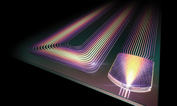
Graphics processing units (GPUs) designed for high-performance computing (HPC) have recently seen dramatic performance improvements driven by the needs of artificial intelligence. The same hardware advances, it turns out, can also serve to significantly speed up numerical simulations of physical phenomena.
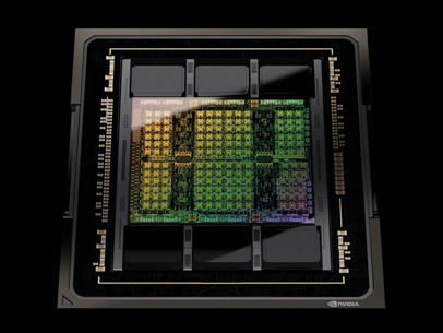 NVIDIA H100 GPU. [NVIDIA]
For problems in optics, one of the best-established numerical techniques for solving Maxwell’s equations is the finite-difference time-domain (FDTD) method. The FDTD method is relatively simple to implement; it is based on first principles and fully vectorial; its computational cost scales linearly with each of the dimensions of the system; and a single simulation can obtain information across a wide electromagnetic spectrum. FDTD is employed in a vast array of applications and has become one of the tools of choice for optics and photonics design across many industries.
Increases in simulation speed enabled by advances in graphic processing units (GPUs) can dramatically reduce the turnaround time of device design and optimization.
The popularity of the FDTD method, however, has also created a need for simulating increasingly larger and more complicated systems, as new devices similarly become ever more complex. Fortunately, the advances in GPU performance are well timed, and the increases in simulation speed they are enabling are both making such large-scale simulations possible and dramatically reducing the turnaround time of device design and optimization. This feature looks at how hardware GPUs are enabling a new era of photonic simulations.
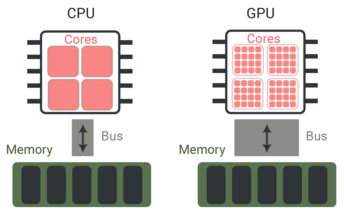 [Enlarge image]A highly simplified schematic comparison of CPU (left) and GPU (right) architectures. The illustration intentionally neglects many complexities to highlight the fundamental similarities and differences between the two platforms.
The GPU hardware advantage
A highly simplified comparison of central processing units (CPUs) versus GPUs provides a convenient entry point for understanding the advantages and limitations of a GPU FDTD implementation. For purposes of this simplified discussion, both architectures have two key components.
The first component is a compute unit, made up of some number of compute cores that can perform floating-point operations. A CPU typically has a much smaller number of cores than a GPU. On the other hand, a core in a CPU is also much more general-purpose than a GPU core, and CPU cores can easily switch between different instructions. GPUs, in contrast, are less flexible, but are great at pushing the same instruction through a very large number of cores. Advances in programming languages and compilers (for example, NVC++) mask the underlying hardware discrepancies and enable acceleration of standard C++ code on GPUs with no language extensions or nonstandard libraries.
In both cases, the number of cores limits the maximum possible throughput of floating-point operations per second (FLOPS). The number of FLOPS, however, is relevant only to the best-case core utilization; in practice, often only a fraction of this throughput will actually be achieved. Therefore, GPUs only outperform CPUs on tasks which parallelize well—that is, which can utilize all cores efficiently.
The second key component of both CPUs and GPUs, which can be a bottleneck for efficient parallelization, is the memory access. Both architectures need to read user inputs from and write results to some form of random-access memory. To support their larger number of cores, GPUs usually need a larger memory bandwidth than CPUs. And for FDTD simulations, the memory bandwidth turns out to be the defining factor for performance.
Modeling FDTD performance on GPUs
With that schematic comparison of hardware architectures as background, we can now use a simple model to compare the expected performance of FDTD simulations on different platforms.
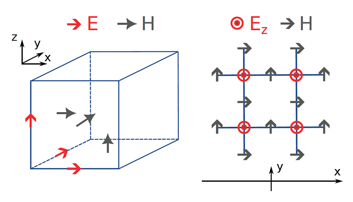 [Enlarge image]Left: The Yee grid for FDTD simulations of Maxwell’s equations, and the locations of the various vector field components which are stored and updated during the execution of the algorithm. E, electric-field component; H, magnetic-field component. Right: 2D cross-section of the Yee grid. In the time stepping, a field component (for example, Ez) is updated using the surrounding four components of the opposite field (for example, Hx and Hy).
In the case of solving Maxwell’s equations for optical simulations, the FDTD method consists of defining the electric (E) and magnetic (H) fields on a finite spatial grid, and repeatedly updating one field using the values of the other. This is ubiquitously done on the so-called Yee grid, in which E is updated from the curl of H, and vice versa (see diagram at upper right). A single cell of a Yee grid contains six components, three for E and three for H; the entire cell is considered updated when all six components have been updated. A common figure of merit for the FDTD execution speed is the number of cells that can be updated per second.
We can predict the FDTD simulation performance on specific hardware with a simple model with two input parameters: the maximum achievable FLOPS (F) and the maximum achievable memory bandwidth (B, measured in bytes per second). If Nfl is the number of operations needed to update a single grid cell and Nbw is the number of bytes that must be read or written to memory during that update, the time needed to perform each function is Nfl/F for the grid cell update (the compute time) and Nbw/B for the memory operation (the bandwidth time).
On practically every modern architecture, memory access and computational operations can overlap, so the time needed to fully update the cell is not the sum of the compute and bandwidth times, but rather just the maximum of the two. Thus, a simple formula for the achievable speed (S) of the FDTD algorithm in cell updates per second is S = min (F/Nfl , B/Nbw).
For the most basic FDTD updates—for example, homogeneous nondispersive materials with no perfectly-matched-layer (PML) boundaries—we can count six floating-point operations (addition or multiplication) to update a single field component, so Nfl = 36 (that is, six components each requiring six operations). Similarly, on the bandwidth side, a single field component would require five reads (the field and the four neighboring components of the opposite field) and one write (the updated field), or a total of six memory access operations; with six field components in total and a size of 4 bytes for single-precision numbers, Nbw = 144 bytes. (While we have assumed single precision here, the same principles apply with similar conclusions using other arithmetic.)
 [Enlarge image]Speed, in billions of cells per second (Gcells/s), versus available memory bandwidth and FLOPS, for several common CPU and GPU chips. Theoretical values have been obtained from manufacturer hardware specifications. The figure is qualitative only; the exact achievable FLOPS and bandwidth can vary significantly depending on application and algorithm implementation. The dashed black line separates bandwidth-limited (above left) and compute-limited (below right) performance.
Running the speed test
We can now compare the model-predicted FDTD speed on different hardware platforms. The comparison, shown in the chart to the right, conveys two important messages. The first is that the FDTD algorithm is strongly bandwidth-limited regardless of hardware. The second is that GPUs—because of their much larger bandwidth—still significantly outperform CPUs.
Even a desktop GPU, such as the NVIDIA RTX 3080, can outperform some of the best CPUs typically found in HPC servers (AMD EPYC 9734, Intel Xeon Max 9462). And, at least for FDTD simulations, the performance difference between the best HPC GPUs (NVIDIA A100 SXM, NVIDIA H100 SXM) and some of the best desktop CPUs (AMD Ryzen 7950X, Intel i9-13900K) approaches some two orders of magnitude.
To go beyond theory, we used Tidy3D, Flexcompute’s implementation of the FDTD method, to measure the achieved performance on several different GPU chips. We found very good agreement with the simple model presented here. We tested a basic FDTD simulation containing a homogeneous nondispersive medium and no PML, and recorded speeds up to 20 Gcells/s on an NVIDIA A100 SXM GPU and up to 33 Gcells/s on an H100 SXM GPU, compared with the model predictions of 14 Gcells/s and 23 Gcells/s, respectively. The FDTD throughput is projected to reach more than 100 Gcells/s on a B200 Blackwell GPU.
The achieved performance was actually higher than predicted, because our simple model neglected the memory hierarchy present in all hardware, which enables caching of data for significantly quicker access. This is also why the exact speed in the experimental benchmarks depends nontrivially on some of the simulation parameters, like the number of grid points along each dimension.
The use of GPUs for FDTD simulations is ushering in dramatic speed increases, with simulation turnaround times one or two orders of magnitude shorter than with conventional hardware.
In some cases—for example, when the GPU is underutilized by small simulations, or the cache is oversaturated for large ones—the recorded speed can also be lower than the prediction. However, we stress that the model presented here has the benefit of being extremely simple and easy to understand intuitively, while still capturing the GPU speed to within a factor of about 1.5 on several different chips and for varying simulation domains. This justifies its use as a credible figure of merit.
New horizons in speed and scale
The use of GPUs for FDTD simulations is ushering in dramatic speed increases, with simulation turnaround times one or two orders of magnitude shorter than with conventional hardware. A single high-end GPU can, within minutes, perform simulations that would have taken hours on a high-end CPU. That speed advantage directly translates into an advantage in scale: For the same simulation time, a much larger, more complex device can be simulated on a GPU than on conventional hardware. This scale advantage is magnified when multiple GPUs work together on a single simulation. This has made it possible to simulate devices that were until recently thought impossible for full-wave methods.
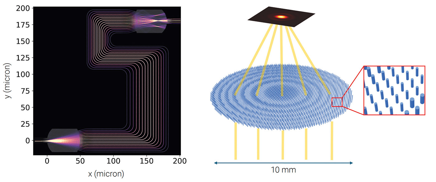 [Enlarge image]Running FDTD models of an arrayed waveguide grating (left) and a metalens (right) on GPU hardware resulted in significant decreases in simulation time. [Flexcompute]
Two such simulations, performed using Tidy3D and 32 A100 GPUs working together, illustrate the point. The first one is a large-footprint (220 × 220 µm) arrayed waveguide grating (AWG) device for a photonic integrated circuit, for use in narrowband wavelength multiplexing. The full 3D simulation, involving 3 billion grid points and more than 300,000 timesteps, was accomplished in just under an hour.
The second example is a large-footprint (10.6 × 10.6 mm) mid-IR metalens (radius 5.3 mm) with a central wavelength of 10.6 µm and a diameter of 1,000 cylindrical-pillar meta-atoms (574,775 meta-atoms in total). This surface was discretized into more than 9 billion grid points, but required only 10,000 time steps to complete, because the device does not have strong resonance and the propagation distance, which is perpendicular to the device, is relatively short. The FDTD simulation time for this metalens design case was only about 7 minutes.
These are just two examples that highlight the paradigm shift in large-scale design engineering using first-principles simulations that GPU advances have made possible. Previously, such simulations would have been too slow, and consequently approximate methods were used—which sacrifice the accuracy of the results.
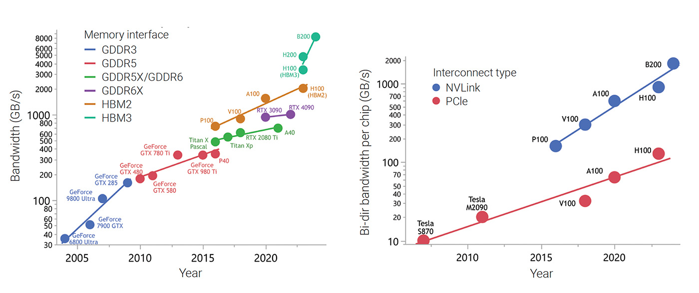 [Enlarge image]Scaling of GPU-to-device-memory bandwidth (left) and GPU-to-GPU bandwidth (right) for different interfaces. [NVIDIA]
Bandwidth on the rise
In the past 20 years, GPU memory bandwidth has increased by about 240 times, which is equivalent to a compound annual growth rate of 32%. Such scaling is driven by higher data transfer rates and wider buses.
GPU-enabled simulations may aid the design of GPU-to-GPU optical interconnects that further push attainable bandwidths—and further improve the scale of the simulations themselves.
In the case of graphics dynamic random-access memory (GDDR), for example, data transfer rate increases with higher clock frequency, at the cost of signal integrity and power consumption. As it becomes more difficult to boost clock frequency to greater than 2.0 GHz, GDDR5X/GDDR6 doubles the data transfer rate by doubling the number of memory reads/writes in each clock cycle. GDDR6X further doubles the data transfer rate by encoding two bits of information in each symbol with PAM-4 signaling.
As the scaling of the GDDR interface slows down, the high-bandwidth memory (HBM) interface carries on with wider buses. If the GDDR interface is like a high-speed train, then the HBM interface is more like a ferry that runs slower but with an order of magnitude or more greater carrying capacity. Each HBM chip has a bus width of 1024 bits, which is 32 times wider than a GDDR chip. Hence a GPU packed with 8X HBM chips, like the NVIDIA Blackwell B200 GPUs used in HGX B200, has a bus width of 8192 bits, which is 16 times wider than a GDDR interface with a 512-bit bus.
For a single GPU, the bandwidth-to-device memory (upper chart on p. 49) determines the speed of an FDTD simulation. On the other hand, the absolute fastest a simulation can run given unlimited hardware resources is determined by the GPU-to-GPU interconnect bandwidth (lower chart on p. 49). Scaling of this bandwidth in recent years has followed a similar trend: the compound annual growth rate is approximately 16% for the PCIe interface, and 32% for NVIDIA’s NVLink interface.
Spinning the wheel of innovation
Increasing device memory bandwidth and GPU-to-GPU bandwidth is dramatically expanding the speed and scale of photonic simulations. Interestingly, many applications of these simulations will also relate directly to hardware advances that will further push the attainable bandwidths. Optical interconnects are becoming increasingly miniaturized and, while they are already ubiquitous for long-range data transfer, are also becoming relevant at shorter and shorter distances.
It is expected that the exponential growth of GPU-to-GPU bandwidth will eventually be continued by optical rather than electronic interconnects (see “Photonics and AI,” p. 26). In the long run, even the single-GPU HBM could end up optically connected. There is already vigorous research and development in both of these directions, requiring a substantial amount of simulation in the design process. And these developments might one day further improve the scale and throughput of the optical simulations themselves—creating a magnificent closed loop of innovation.
We thank Prashanta Kharel and Xinzhong (Tom) Chen for development of the AWG and metalens examples shown in this article, and Tyler Hughes, John Moore and Emerson Melo for insightful discussions.
Momchil Minkov is with Flexcompute, Watertown, MA, USA. Zongfu Yu is with Flexcompute and the University of Wisconsin, Madison, WI, USA. Shanhui Fan is with Flexcompute and Stanford University, CA, USA. Peng Sun and Ben Lee are with NVIDIA Corp., Santa Clara, CA, USA.
References and Resources
-
A. Taflove and S. C. Hagness. Computational Electrodynamics: The Finite-Difference Time-Domain Method, 3rd ed. (Artech House, Norwood, 2005).
-
T.W. Hughes et al. Appl. Phys. Lett. 119, 150502 (2021).
-
F. Teixeira et al. Nat. Rev. Methods Primers 3, 75 (2023).
