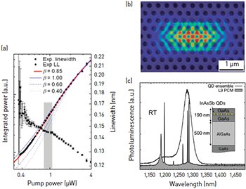
 (a) Integrated power emitted by laser versus pump power and theoretical curve fits for different β values. (b) Calculated spectral distribution of lasing mode superimposed on SEM image of the photonic-crystal microcavity (PCM). (c) Photoluminescence spectrum of the ensemble of QDs outside (black line) and inside (grey) of the PCM, at room temperature. Inset describes the layers that compose the device.
The laser semiconductor industry is growing at a rate of some 7 percent per year, with revenues expected to reach more than US$7.7 billion by 2020. This expansion is driven by applications that benefit from the compact size and low cost of these lasers. Their efficiency is also improving—but it is still far from optimal. Typical laser thresholds— that is, the point at which the optical output changes from spontaneous to stimulated emission—are still high. That, in turn, results in high energy consumption, as laser pumping power is largely devoted to spontaneous-emission photons rather than lasing (stimulated-emission) photons.
Lowering the laser threshold would allow significant power savings to drive laser-based devices, and facilitate global energy savings when multiplied by the millions of semiconductor laser devices deployed worldwide. Consequently, thresholdless lasers have been a holy grail since the laser’s invention. Earlier this year, we demonstrated a near-thresholdless laser that operates at room temperature.
Today, the term thresholdless is defined as a device with high-rate lasing to spontaneously emitted photons (called the β factor, with a value between 0 and 1) and low nonradiative losses.1 The key elements in fabricating such a device have been envisioned as a combination of high-efficiency light emitters such as quantum dots, and high-quality optical resonators like photonic-crystal microcavities.1 This approach was used previously to achieve ultra-low-threshold lasing (β=0.85), but at low temperatures (4.5 K).2 While an important leap forward, the need for cryogenic temperatures prevents the feasibility of this approach in standard consumer laser products.
The laser was based on indium arsenide antimonide (InAsSb) QDs placed in a photonic crystal microcavity emitting in the wavelength of 1,286 nm at room temperature.3 The laser exhibited an ultra-low power threshold (860 nW) and high-efficiency (β=0.85) values at room temperature, thus operating in the near-thresholdless regime. Although the demonstrated device is optically pumped, electrically injected versions are possible when following a similar approach. The results open up a wide range of opportunities for room-temperature applications and ultra-low-threshold lasers, such as integrated photonic circuitry or high-sensitivity biosensors.
Researchers
I. Prieto and A.G. Taboada, IMM–Instituto de Microelectrónica de Madrid, Spain, and ETH Zurich, Switzerland
J.M. Llorens, L.E. Muñoz-Camúñez, J.M. Ripalda, C. Robles and P.A. Postigo, IMM–Instituto de Microelectrónica de Madrid
G. Muñoz-Matutano, UMDO (Unidad asociada al CSIC) and ITEAM, UPV, Valencia, Spain
J.P. Martínez-Pastor, UMDO (Unidad asociada al CSIC)
References
1. S. Noda. Science 314, 260 (2006).
2. S. Strauf et al. Phys. Rev. Lett. 96, 127404 (2006).
3. I. Prieto et al. Optica 2, 66 (2015).
