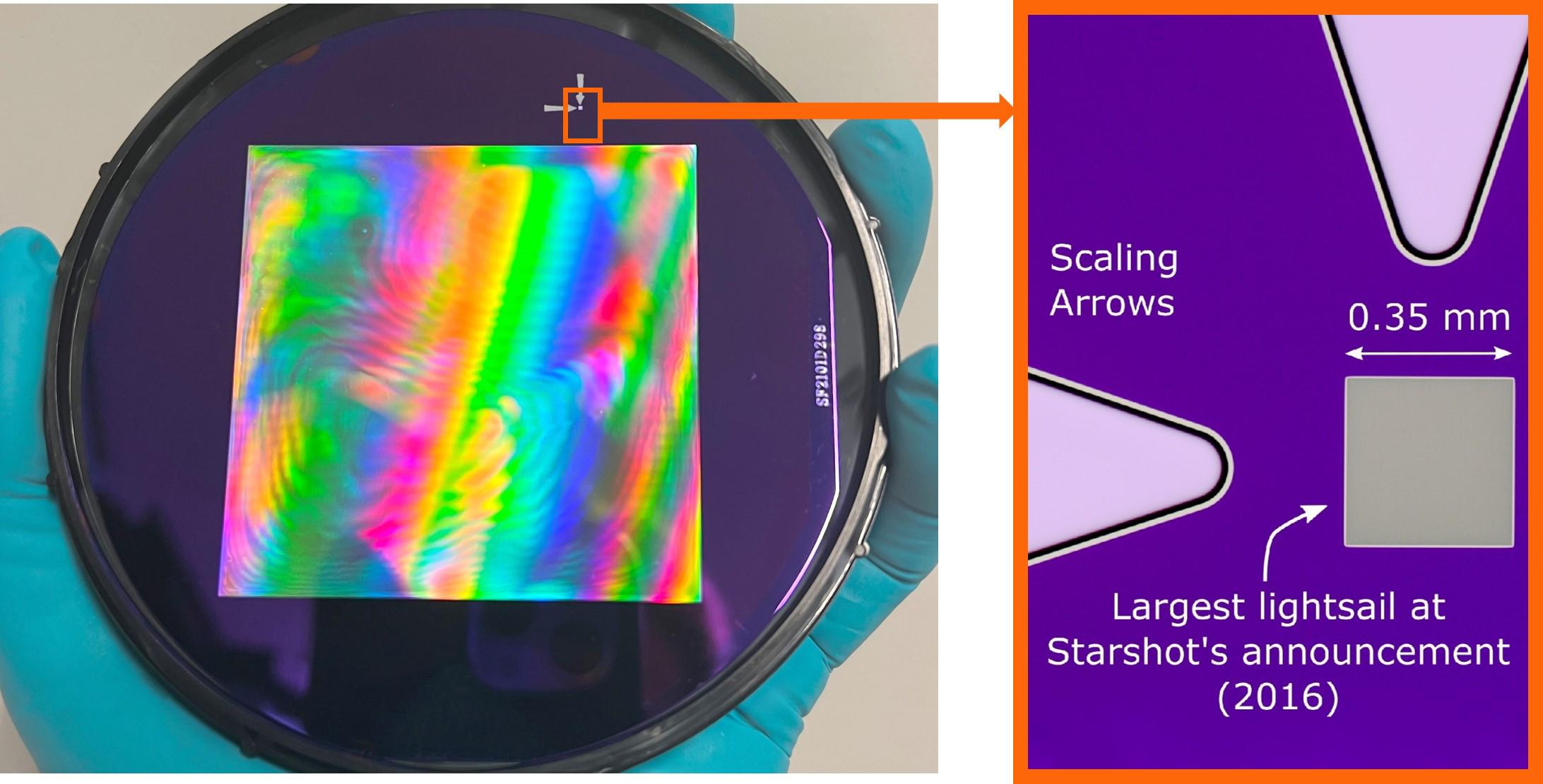
Researchers have designed and fabricated a silicon nitride lightsail measuring 6 cm by 6 cm by 0.2 µm. [Image: Richard Norte]
The Starshot Initiative has the ambitious aim of sending spacecraft to Alpha Centauri—the nearest star beyond the solar system—in flights lasting just 20 years. They plan to achieve this feat by using very intense laser beams fired from Earth to propel exceptionally thin “lightsails.”
Researchers in the Netherlands and the United States have now developed a possible blueprint for such sails (Nat. Commun., doi: 10.1038/s41467-025-57749-y). The team showed that 200-nm-thick sheets of silicon-nitride photonic crystal with billions of tiny holes arranged in a pentagonal lattice could provide the necessary performance at an affordable cost.
Reaching for the stars
Entrepreneur Yuri Milner and the late physicist Stephen Hawking launched the Starshot Initiative in 2016 to try and slash the journey times of interstellar travel. Voyager 1, launched in 1977, recently left the solar system and is currently more than 15 billion miles from Earth, but it would take at least another 10,000 years to go as far as Alpha Centauri.
The initiative envisages using laser beams with intensities of several gigawatts/m2 to accelerate lightsails with microchip-based payloads to about a fifth of the speed of light in only around 10 minutes. Then, the beams would turn off to let the objects travel unimpeded at that speed through interstellar space. The sail would absorb very little of the incident light, instead reflecting it to provide an impulse in the direction of the light’s propagation.
The alternating refractive indices across the plane transform the optical mode of incoming light so that it interferes destructively with transmitted waves but constructively with reflected ones.
Among the biggest challenges in realizing this ambition is manufacturing lightsails with dimensions that provide the necessary propulsion while weighing only about 1 g. As Richard Norte and colleagues at the Delft University of Technology, Netherlands, point out, the payload—comprising miniaturized cameras, sensors and other probes—would have a small size in all three dimensions, whereas the sails must have a macroscopic area—about 10 m2—but micro- or nanoscale thickness, which implies an aspect ratio of 100,000 or more.
Thinner, lighter and cheaper
In the latest work, Norte, Lucas Norder and colleagues in Delft have joined forces with Miguel Bessa and Shunyu Yin at Brown University, USA, to make sails from low-density, low-absorption and high-reflectivity silicon nitride. In principle, sails could be composed of multiple layers of photonic crystal to form distributed Bragg reflectors with very high, broadband reflectivity, but they would weigh several hundred grams for a 10 m2 area.
Instead, the researchers employed a single layer of photonic crystal consisting of a two-dimensional array of holes. The alternating refractive indices across the plane transform the optical mode of incoming light so that it interferes destructively with transmitted waves but constructively with reflected ones.
Unlike previous groups that focused above all on flight performance, Norte, Bessa and coworkers also looked to minimize manufacturing costs. They did so by stipulating feature sizes of no more than 500 nm, which aids manufacturing and reduces breakages, although also limits acceleration. In particular, they were able to use high-throughput optical lithography rather than much slower electron lithography, saving on clean-room costs.
With regards to performance, the team focused on reducing powered flight time. Although powered flight is foreseen to last only a few minutes, the enormous laser power involved implies electricity bills of millions of US dollars per launch. With potentially hundreds of such devices being put into space, the researchers say that minimizing laser usage could bring huge savings.

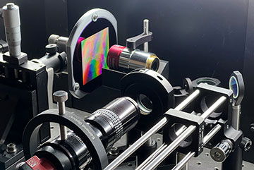
Membrane held in the measurement setup [Image: Richard Norte]
Toward firing through space
Using a technique known as neural topology optimization, Bessa and Yin settled on a design featuring a pentagonal lattice of irregularly shaped holes occupying about 60% of the sail’s area. The variation in hole size should yield a number of peaks in the sail’s reflectance spectrum, reducing overall reflection compared with other shapes but crucially extending the device’s bandwidth. This should ensure that sails can continue to reflect the (monochrome) laser light as it becomes Doppler shifted due to the spacecraft’s increasingly great speed.
With the design settled on, Norte and colleagues set about producing the physical object—a 6-cm-long, 6-cm-wide, 0.2 µm-thick silicon nitride membrane fabricated on top of a 10-cm-diameter silicon wafer. The process involved depositing and then carving up the silicon nitride before using a novel gas-based etching technique to remove a layer of silicon from beneath, which left the sail suspended above the remaining substrate.
The researchers then recorded the device’s reflectivity spectrum with a mixture of infrared measurements and simulation, confirming the expected performance bar slight variations caused by excessive etching of the silicon nitride and fractionally larger holes at the edge of the sail. Norte and colleagues argue that their scheme ought to yield suitable lightsails using any sized semiconductor wafer, having shown that such devices “can be produced in a truly scalable manner by optimizing both manufacturing costs and design.”
The researchers’ next steps include scrutinizing sails’ thermal stability, compatibility with payloads and performance at very high laser powers. However, actually firing such sails through space will take more time. To date, radiation pressure has been used to nudge similarly thin sails by no more than about the diameter of an atom. Norte and his group are now preparing experiments to displace their own (larger) sails by around a centimeter, which he says they hope to do “within the next few years.”

