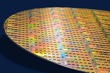
A silicon photonics wafer full of Ayar Labs' "TeraPHY" optical I/O chiplet devices. [Image: Ayar Labs]
On 11 December 2024, optical-interconnect solutions provider Ayar Labs, USA, announced that it had received an investment of US$155 million from three leading US-based chip manufacturers—AMD Ventures, Intel Capital and NVIDIA—to support its work using light to transmit data between chips. Led by Advent Global Opportunities, UK, and Light Street Capital, USA, this latest infusion of series D funds put Ayar Labs into rare “unicorn” territory as a privately held startup with a total valuation exceeding US$1 billion.
AI leads the way
This development is yet another indicator of the frenzy within the industry to find fiber optic solutions for enabling bandwidth-guzzling artificial intelligence (AI), as traditional copper wires rapidly run out of length. Indeed, according to a recent Goldman Sachs report, tech firms, corporations and utilities are poised to spend in the neighborhood of US$1 trillion on capital expenditures to support AI in the next decade.
“The leading GPU providers—AMD and NVIDIA—and semiconductor foundries— GlobalFoundries, Intel Foundry and TSMC—combined with the backing of Advent, Light Street and our other investors underscores the potential of our optical I/O [input/output] technology to redefine the future of AI infrastructure,” said Mark Wade, CEO and cofounder of Ayar Labs, in a press release.
Other investors that participated in the latest funding round include 3M Ventures, USA, and Autopilot, USA. They join existing investors Applied Ventures LLC, Axial Partners, Boardman Bay Capital Management, GlobalFoundries, IAG Capital Partners, Lockheed Martin Ventures, Playground Global and VentureTech Alliance, all of which are based in the United States.
Like co-packaged optics (CPO) ... optical interconnects hold promise for delivering higher bandwidth, lower power consumption, lower latency and longer reach compared with traditional electrical setups.
Optical I/O interconnects
Ayar Labs’ work focuses specifically on optical I/O interconnects, which use “chiplets,” or miniaturized integrated circuits, to transfer light signals between and within chips. Like co-packaged optics (CPO), another technology receiving industry attention, optical interconnects hold promise for delivering higher bandwidth, lower power consumption, lower latency and longer reach compared with traditional electrical setups. Yet the two concepts are different: CPO refers to a broad strategy for integrating optical components into the same package as the electronic chip, while optical I/O interconnects create direct connections between chips at the board, rack or system level.
Founded in 2015, Ayar Labs claims to have developed the industry’s first in-package optical I/O solution to replace electrical I/O that is standards-based, commercial-ready and optimized for AI training and inference.
Soaring growth in silicon photonics
Nvidia also participated in Ayar Labs’ earlier funding rounds. The company’s continuing investment suggests the chip-making giant is looking to supply the burgeoning generative-AI area. With year-to-date market growth of almost 195% as of late November 2024, Nvidia has nearly tripled in value over the past 11 months.
Meanwhile, several other privately held companies focused on optical-interconnect technologies, including Celestial AI, USA; Quintessent, USA; and Oriole Networks, UK, have also raised significant equity funding this year. In addition, Celestial AI recently announced the acquisition of silicon photonics intellectual property (IP) from Rockley Photonics, UK.
Not surprisingly, a new report from Yole Group shows the silicon photonics market as a whole is accelerating rapidly. It is projected to increase from US$95 million in 2023 to more than US$863 million in 2029, with a compound annual growth rate of 45%.
