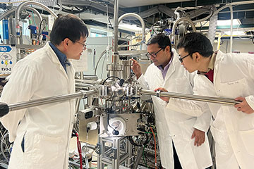
Zhifei Yang (left), Bharat Jalan (center) and Fengdeng Liu have shown that heterostructures made from interleaved layers of doped and undoped strontium tin oxide yield high conductivities while also being transparent to deep-ultraviolet radiation. [Image: Kalie Pluchel / University of Minnesota]
Researchers in the United States have found that structures made from very thin slices of specific oxides demonstrate two qualities crucial for future semiconductor devices―being both highly conductive and transparent at deep-ultraviolet wavelengths (Sci. Adv., doi: 10.1126/sciadv.adq7892). They say that their ultrawide-bandgap heterostructures would be well-suited to a range of applications requiring electronics to operate at high temperatures.
Transparent conducting oxide
Semiconductor manufacturers are continually looking to improve the performance of their devices, including those that need to be transparent at certain wavelengths. To this end, researchers are currently investigating what are known as transparent conducting oxides, which can be used to make electrodes for light-emitting diodes operating in the deep ultraviolet―and which could as a result be incorporated into aerospace detectors, biomolecular sensors and devices for controlling pathogens in food and water.
Two widely used transparent conducting oxides are aluminium-doped zinc oxide and silicon-doped indium oxide. However, these materials are not ideal for very short wavelengths. They have bandgaps of 3.3 electronvolts (eV) and 3.7 eV, respectively, compared with the energies of at least 4.1 eV that are characteristic of the deep ultraviolet. Strontium tin oxide (SSO) instead has a bandgap of 4.1 to 4.2 eV, as well as a high conductivity (of around 3000 siemens per centimeter).
Looking for net electron transfer
In the latest work, Bharat Jalan and graduate students Fengdeng Liu and Zhifei Yang, University of Minnesota, working with colleagues in Minnesota and at the California Institute of Technology, looked to improve the electron mobility of SSO at room temperature through suitable doping. Their structure consists of a 4-nm-thick layer of SSO sitting atop a 19-nm-thick layer of lanthanum-doped SSO that they grew on a substrate of gadolinium scandium oxide.
The researchers predicted that there should be a net transfer of electrons within the structure, from the doped to the undoped layer of SSO. This, they say, means that charge carriers become separated from their dopants, reducing scattering and so boosting mobility and conductivity.
To confirm this prediction experimentally, Jalan and coworkers made a series of heterostructures in which the layer of lanthanum-doped SSO, rather than being uniform, consisted of seven doped sub-layers interleaved with seven undoped sub-layers. When the researchers varied the relative thickness of the two types of sub-layer, they found that as they increased the thickness of the undoped sub layers, the conductance of the structure dropped off more quickly than predicted by a simple model in which conducting electrons emerge only from doped sub-layers. They say that this result supports the idea that electrons diffuse from the doped sub-layers to the undoped ones.
When the researchers varied the relative thickness of the two types of sub-layer, they found that as they increased the thickness of the undoped sub layers, the conductance of the structure dropped off more quickly than predicted by a simple model.
Adjusting electron density
With this demonstration in the bag, the researchers then showed they could adjust the density of electrons in the undoped layer in two ways. One option is to vary the degree of doping in the doped layer. The other is to use what is known as electrostatic gating, which involves placing an ion gel in contact with the undoped layer to generate very high electric fields at this interface, forcing additional electrons up from the doped layer.
In this way, the researchers found that they could yield the equivalent of as many as 1020 electrons for each cm3 of undoped SSO. They also demonstrated electron mobilities of up to 140 cm2 V−1 s−1 at room temperature, which they point out is twice as high as the previous best in doped SSO.
The team was able to reproduce these results by calculating electron–phonon interactions and phonon-limited mobilities at room temperature from first principles. They say that this suggests it should be possible to further boost electron mobility at room temperature by increasing the density of electrons (which screens electron–phonon scattering).
As for transparency, Jalan and colleagues found that their sample transmitted 85% of the deep ultraviolet radiation directed at it. They conclude that their research demonstrates the potential of using heterostructures to build devices from ultrawide-bandgap semiconductors. The researchers point out that the use of ultrawide bandgaps boosts performance at high temperatures, which makes such materials ideal for electronics that have to operate in hot, harsh environments.
