
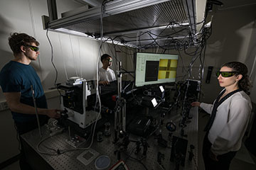
Andrea Pickle (right), Benjamin Harrington (left) and Ziyang Ye in Pickle's lab developing new techniques for mapping heat transfer in electronic devices. [Image: University of Rochester photo / J. Adam Fenster]
Scientists in the USA have shown how to carry out optical thermometry in the far field at resolutions below the diffraction limit by using two different lasers to excite and suppress fluorescence from nanoparticles containing ytterbium and thulium (Sci. Adv., doi: 10.1126/sciadv.ado6268). They say that their technique, which takes temperature readings on scales of just over 100 nm, could be used to improve the performance of electronic devices and study the breakdown of classical heat transfer.
How to map temperature in the nanoscale?
Smartphones, laptops and other modern electronic devices rely on nanometer-sized transistors to yield high performance from small volumes, meaning that overheating is an ever-present risk. But when thermal failure does strike, establishing exactly what has gone wrong is a tricky task―given the difficulty of making reliable temperature measurements on the nanoscale.
Temperature mapping with spatial resolutions below 100 nm can be carried out using methods that rely on physical contact, such as scanning thermal microscopy, or on techniques that exploit the near field. But in these cases the probe itself can thermally interfere with the sample. Conversely, far-field techniques avoid such interference but are diffraction-limited to resolutions of no better than several hundred nanometers.
Reaching super-resolution
An alternative approach, optical super-resolution imaging, combines far-field optics with resolutions beyond the diffraction limit, and has enjoyed much success in biomedical studies. This method comes in a number of different forms, including one called stimulated emission depletion microscopy (STED). This involves directing two separate lasers at a group of fluorescent molecules; one laser excites the molecules, and the other stimulates the excited molecules so that only a fairly small fraction actually fluoresce (the others instead emit in the infrared). With the second (“depletion”) beam having a doughnut shape, an otherwise quite large emitting volume can be made much smaller, thereby boosting resolution.
In the latest work, researchers at the University of Rochester, NY, adapt super-resolution imaging for use in physical-science applications rather than biomedical systems.
In the latest work, Andrea Pickel and colleagues at the University of Rochester, NY, adapt this technique for use in physical-science applications rather than biomedical systems. Instead of using a lens immersed in oil and positioned within a millimeter of the sample, they employ a lens separated from the sample by about a centimeter. That sample consists of upconverting nanoparticles―roughly 130-nm-diameter hexagons made from sodium yttrium fluoride that are doped with ytterbium and thulium ions. The former absorb light from the excitation laser; the latter luminesce and have that luminescence suppressed.
Using just the 976-nm-wavelenth excitation laser to image a single nanoparticle on a borosilicate glass substrate, the researchers obtained an intensity profile about 460 nm wide. In contrast, by shining both that and the 808-nm-wavelength depletion laser at the target simultaneously, they ended up with an image just 136 nm wide―a scale that they say could be reduced when using smaller particles.
The researchers also carried out spectroscopy, recording emission spectra from an individual nanoparticle held at room temperature 293 K, 350 K and 400 K. They identified a number of peaks in the spectrum, including one at about 490 nm that became more pronounced at the higher temperatures. They went on to exploit this temperature dependence by comparing the emission intensity from this peak to that of another at 515 nm, which remains essentially static as the temperature rises.
Putting the nanoscale thermometer to the test
Carrying out a number of tests to confirm the system’s suitability as a nanoscale thermometer, Pickel and colleagues confirmed that the spectrum at each temperature was the same whether using STED imaging or its more straightforward confocal counterpart. They also obtained similar results from both isolated single nanoparticles and from a whole layer of particles―as would be needed when doing mapping. Using band-pass filters and an avalanche photodiode, they were able to record temperature-dependent maps of the 490-nm:515-nm intensity ratio in under a minute. Those maps, which should have been uniform, featured spatial variations of about 10 K, which the researchers put down to slight variations in the fabricated nanoparticles.
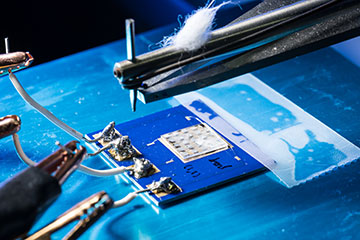
Researchers have developed a new way of mapping temperature variations on the nanoscale that involves using two different lasers to reduce the emission profile from upconverting nanoparticles to below the diffraction limit. [Image: University of Rochester photo / J. Adam Fenster]
Finally, the researchers applied their technique to something approaching a real-life system―snake-like heating lines about 1 micrometer wide and 50 nm thick, made from nickel-chromium alloy on a crystalline quartz substrate. When applying an electrical current, they observed higher current densities and so higher temperatures on the insides of bends than they did on the outsides. They then dropped a cluster of nanoparticles spanning the width of one particular bend, and found that only when carrying out a STED measurement were they able to detect the temperature difference (about 40 K) between the inside and outside of the bend. A diffraction-limited measurement, in contrast, showed no discernable difference in temperature.
“These results,” conclude Pickel and co-workers, “indicate the potential of STED nanothermometry to reveal temperature heterogeneities in microstructures and nanostructures that are undetectable with diffraction-limited optical thermometry.”
The researchers go on to explain that their system could be improved in a number of ways. One possibility, they say, is to tweak the nanoparticle design so that the emission peaks with the strongest temperature dependence are also those with the greatest emission intensity (something that is not the case in the present work). The upshot would either be a higher spatial resolution for given laser powers or the same resolution at lower powers. The latter option, they point out, helps to avoid any laser-induced heating of the samples.
Pickel adds that there are, in principle, a number of ways that they could boost the brightness of their nanoparticles, whether across the emission spectrum or else targeting specific peaks. She says they are currently working to better understand the origin of the temperature-dependent 490-nm peak, and argues that if they can do so, “it’s reasonable to expect that modeling and synthetic strategies could be combined to selectively enhance the temperature-dependent emission.”