
A metalens with a diameter of 100 mm provides the large numerical aperture needed to image astronomical objects such as the moon. [Image: Capassso Lab/Harvard SEAS]
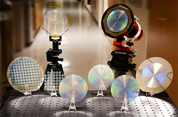
Federico Capasso and colleagues at Harvard University, USA, have fabricated a glass metalens that they say is large enough to image the sun, moon and distant nebulae with high resolution (ACS Nano, doi.org/10.1021/acsnano.3c09462). With more than 18 billion nanostructures patterned onto the surface of the silica substrate, the 100-mm lens operates in the visible range and can be mass produced using standard chip fabrication technologies.
Engineering nanostructures
Metalenses exploit pillar-shaped nanostructures to focus and manipulate light, allowing the function of several optical components to be combined into a single element that is both flat and extremely thin. However, larger metalenses require vast numbers of precisely engineered nanostructures to be fabricated over a wide area, which is impractical to achieve with direct writing tools such as electron-beam lithography.
Capasso and his team showed a few years ago that centimeter-scale metalenses can be produced with deep-ultraviolet lithography, which is most commonly used to manufacture computer chips. Indeed, a spinoff company called Metalenz is now exploiting this approach to produce compact optical elements for applications such as mobile phones, smart robotics and augmented and virtual reality.
Space through a metalens
However, these lithography tools only expose small areas of the substrate at a time, so the researchers devised a method to stitch together multiple parts of the nanopillar pattern. Since the lens has rotational symmetry, they divided the wafer area into 25 sections―one in the middle and six in each of the four surrounding quadrants―that could all be patterned using seven distinct photomasks. First they exposed the central section plus the six sections in one quadrant, and then the substrate was rotated to replicate the pattern in each of the remaining quadrants.
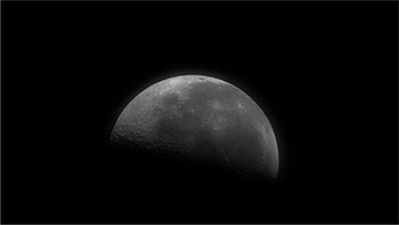
An image of the moon taken by the metalens from the roof of a building in Cambridge, MA. [Image: Capassso Lab/Harvard SEAS]
The fully automated process takes around 20 minutes and produces a metalens about 0.5 mm thick, compared with 21 mm for a normal refractive lens with the same diameter. By optimizing the etching technique used to create the nanopillars, the team also fabricated more vertical structures with smoother sidewalls than previously achieved.
Having fabricated the lens, the researchers combined it with a color filter and camera sensor to capture detailed images of the sun, the moon and the North America Nebula. The team also demonstrated that the optical performance of the lens, which has potential applications in remote imaging, is unaffected by extreme temperatures or the intense mechanical vibrations that occur during a space launch.
