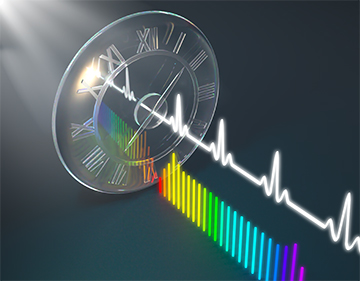
A time lens transforms a continuous-wave, single-color laser beam into a high-performance, on-chip femtosecond pulse source. [Image: Second Bay Studios/Harvard SEAS]
Scientists have long wished for a high-quality ultrafast-pulse source small enough for a chip. However, the tunable femtosecond lasers that provide these light pulses fit on a tabletop, not a semiconductor wafer. Microresonator frequency combs, or “microcombs,” that might otherwise fill the bill have low efficiency and weak pulse energies.
Now, researchers based in the United States have integrated a femtosecond pulse source onto a photonic chip made of lithium niobate, a material with many interesting nonlinear optical properties (Nature, doi: 10.1038/s41586-022-05345-1). To synthesize the ultrafast pulses, the device uses a “time lens”—a temporal analog to a spatial optical system. The resulting source produces trains of 520-fs pulses with energies of 0.54 pJ and a line spacing of 30 GHz.
How the time lens works
A conventional or spatial lens diffracts light and focuses light rays on a focal plane. But spatial diffraction has a mathematical analog: temporal dispersion. Instead of a physical lens, the temporal system takes continuous wave light from a laser chip and runs it through an amplitude modulator, phase modulator and dispersion medium. The first element of the trio shapes the light to fit the temporal “aperture”; the second element chirps the pulses and generates the multi-colored frequency comb; and the third element introduces group delay dispersion (see “Ultrahigh-Speed Optical Processing Using Space-Time Duality,” OPN, May 2011).
Instead of using tabletop components to perform the time-lens manipulations and feeding the resulting pulses into a chip, the team led by Marko Lončar, an electrical engineering professor at Harvard University, crammed all three elements into a 25×4-mm2 footprint on a 600-nm-thick lithium niobate film supported by a 2-μm-thick substrate.
A bevy of potential applications
According to the researchers, the lithium niobate platform developed in the Harvard lab greatly reduces the complexity of the circuitry needed to produce well-controlled femtosecond pulses. “You just get better performance as the device gets smaller and more integrated,” the study’s first author, Mengjie Yu, said in a press release. (Yu was a Harvard postdoctoral fellow at the time of the work; she has since moved to the University of Southern California, USA.)
The researchers predict that the miniaturized femtosecond-pulse source could find a home in applications ranging from optical clocks to lidar and astronomical spectrography. The team hopes to explore its use in quantum networking.
