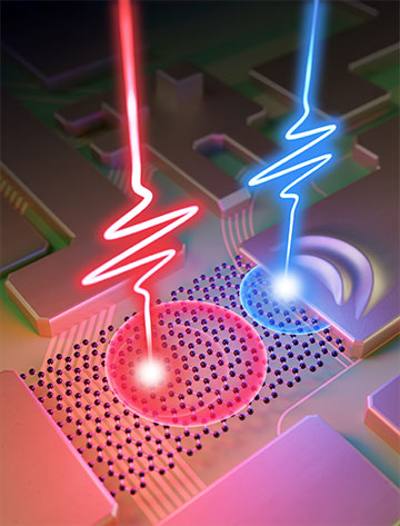
A new type of logic gate sums the electric current from real and virtual charge carriers that are generated by firing two synchronized laser pulses at different portions of a tiny strip of graphene connected to gold electrodes. [Image: University of Rochester illustration / M. Osadciw]
Researchers in Germany and the United States have used ultrashort bursts of intense laser light to create a logic gate that could operate at petahertz clock rates (Nature, doi: 10.1038/s41586-022-04565-9). They did so by independently controlling so-called real and virtual charge carriers. The team argues that its result paves the way to a new form of exceptionally fast information processing based on “lightwave electronics.”
A path to faster logic gates
Logic gates in conventional electronic circuits are made up of transistors, which take about a nanosecond to switch and thereby limit clock rates to frequencies of gigahertz (109 Hz). Lasers, on the other hand, can generate light pulses on timescales of femtoseconds (10–15 s)—meaning that operations could potentially be made a million times faster.
Ignacio Franco put forward a scheme for converting such laser pulses into bursts of electricity in 2007 when he was a Ph.D. student at the University of Toronto, Canada. He proposed making a nanometer-sized junction by connecting carbon-based molecular wire to a pair of metal electrodes. Exposing the wire to femtosecond laser pulses, he reasoned, should shift the carbon’s energy levels enough that a tiny current could flow toward one of the electrodes.
This scheme was demonstrated experimentally six years later by Ferenc Krausz and colleagues at the Max Planck Institute of Quantum Optics in Garching, Germany, who used a slightly different set of materials—placing a glass wire between a pair of gold electrodes. However, this and subsequent studies were not able to pin down the roles played by real and virtual charge carriers in the current-generation process. Both types of charge carriers are electrons, but while the former continue to move with the current flow after the laser pulse has ended, the latter cease directional motion when no longer illuminated.
Creating real and virtual charge carriers
To study the roles of real and virtual charge carriers in detail, Franco, now at the University of Rochester, USA, teamed up with Peter Hommelhoff and colleagues at the Friedrich-Alexander-Universität Erlangen-Nürnberg (FAU) in Germany—this time placing a strip of graphene between gold electrodes. Their key control knob was the phase of the carrier envelope—which quantifies the offset between the peak of a pulse envelope and the carrier wave inside it. To generate real charge carriers, they used a laser pulse whose electric-field peak was out of phase with the envelope by ± π/2. This resulted in the largest difference between the positive and negative peak amplitudes of the light’s vector potential, so imparting the greatest net momentum to the electrons excited from the graphene’s conduction band.
The researchers produced virtual charge carriers, in contrast, by offsetting the electric-field peak by either 0 or π. This type of pulse resulted in the largest possible asymmetry in the spatial distribution of electrons within the material, allowing them to be captured at the graphene-electrode interface while the pulse remained on—thereby contributing to the current flow towards that electrode.

FAU physicist Peter Hommelhoff [Image: U. Niklas / FAU]
Hommelhoff and colleagues demonstrated these two distinct contributions to the electric current by varying the length of their graphene strip (which was 1.8 µm wide) and illuminating its center with 6-fs near-infrared laser pulses. For a 5-µm-long strip, the pulse intensity peak was too far from the electrodes to generate any significant quantity of virtual charge carriers, meaning that the greatest current was generated for a phase offset of ± 3π/2. Conversely, for a strip just 1 µm long, the maximum current occurred at an offset of about 0.9 π. An intermediate length of 2 µm instead yielded a peak at about 3π/4.
Getting to a laser-driven logic gate
To exploit what they have learned for the purposes of logic circuitry, the researchers applied two laser pulses to a single 5-µm strip of graphene. They aimed the first pulse at the middle of the strip, generating real charge carriers that propagated towards one of the gold electrodes. They then arranged the second pulse so that it fired at the interface between the strip and that electrode, synchronizing the pulse’s firing with the arrival of the electrons—so yielding virtual charge carriers (given the right phase) that added to the current.
By passing the first laser pulse through varying thicknesses of a wedge of silicon dioxide, the researchers were able to modify the relative carrier envelope phase of the two pulses. They then set up a truth table by using four appropriate values of the relative phase and specifying that the output current signaled a “1” when above a certain threshold.
In particular, they demonstrated how to set up the truth table for a NOR gate—choosing values of the phase such that only one combination, (0,0), yielded a 1 at the output. But they say that by choosing other combinations of phase it would be straightforward to set up a range of other logic gates, including AND, OR and NAND.
An “initial step”
Hommelhoff is confident that the ultra-short timescales of the illuminating laser pulses can be converted into much higher clock rates than is possible with conventional electronics. But he cautions that there are a number of major hurdles that have to be overcome before the technology can be commercialized. Among these, he says, are scaling up to multiple logic gates while retaining the high operating speeds, as well as shrinking the gates by making use of near-field optics and reducing the pulses’ intensity.
“Much more fundamental as well as applied research is needed to turn this into a new technology,” Hommelhoff says. “But at least the initial step is done now: the demonstration of a new logic gate.”

